Op amp circuit PCB design skills
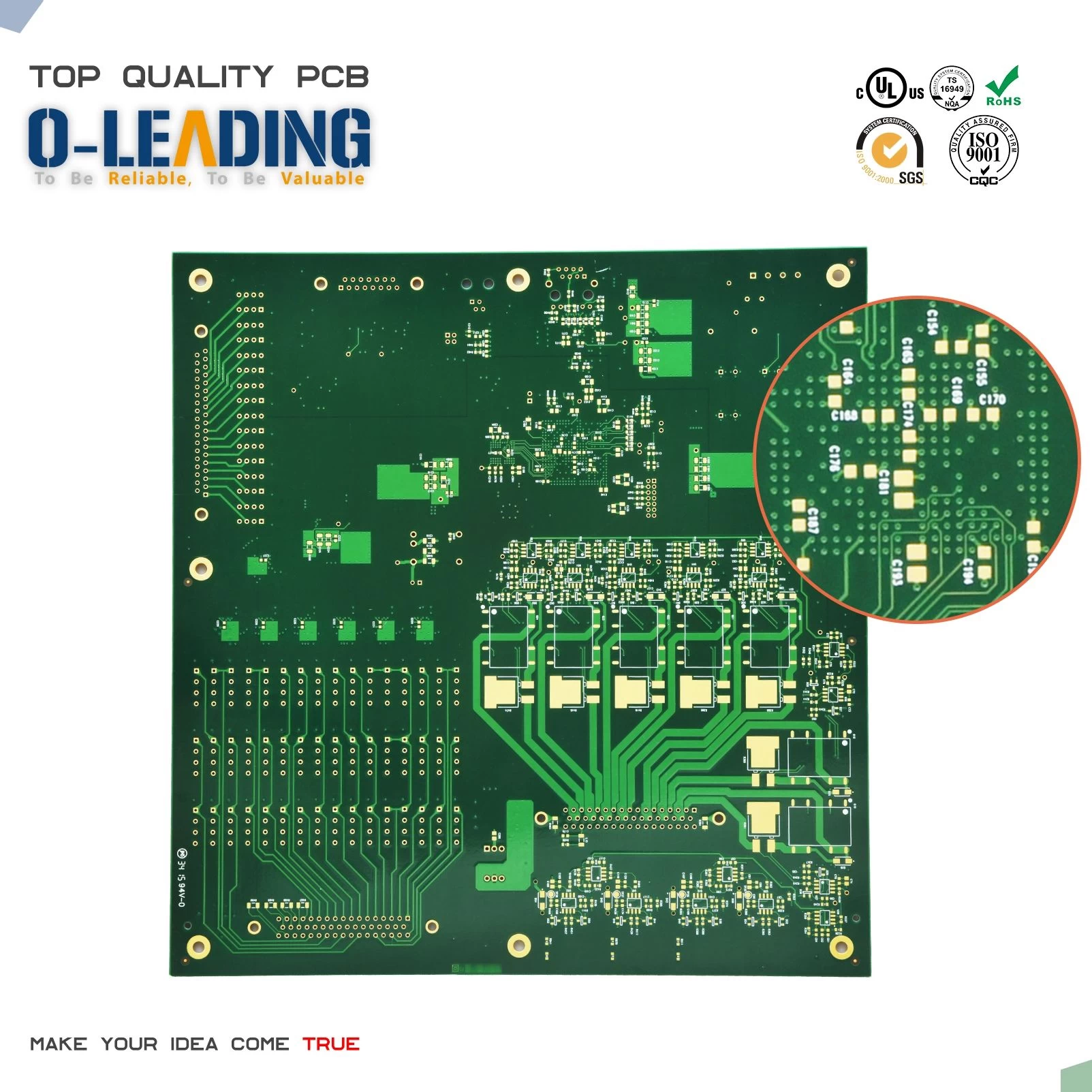
1. In the PCB design, the capacitors such as bypass filter at the chip power supply should be as close as possible to the device, and the typical distance is less than 3MM. Halogen Free PCB manufacturer china.
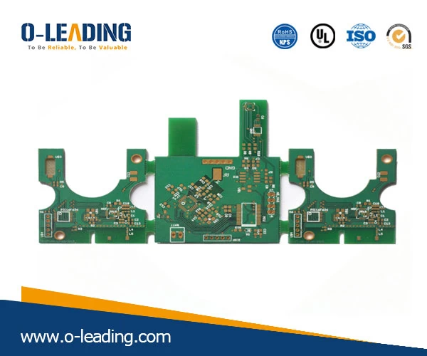
2. The small ceramic bypass capacitor at the power supply of the operational amplifier chip can provide the energy capacitance value for the high frequency characteristic of the amplifier when the amplifier is at the input high frequency signal. According to the frequency of the input signal and the speed of the amplifier, for example, a 400MHz amplifier It is possible to use a 0.01uF and 1nF capacitor installed in parallel.
3. When we buy a device such as a capacitor, we also need to pay attention to its self-resonant frequency. The self-resonant frequency at this frequency (400MHz) has no benefit.
Halogen Free manufacturer china.
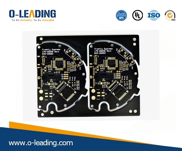
4. When drawing the PCB, the input and output signal pins of the amplifier and the underside of the feedback resistor should not be on other lines, which can reduce the mutual influence of the parasitic capacitance between different lines to make the amplifier more stable.
5. The high-frequency new energy of the surface mount device is better and smaller.
6. When wiring the board, keep the trace as short as possible while paying attention to his length and width to minimize parasitic effects.
Controlled impedance PCB supplier in china.
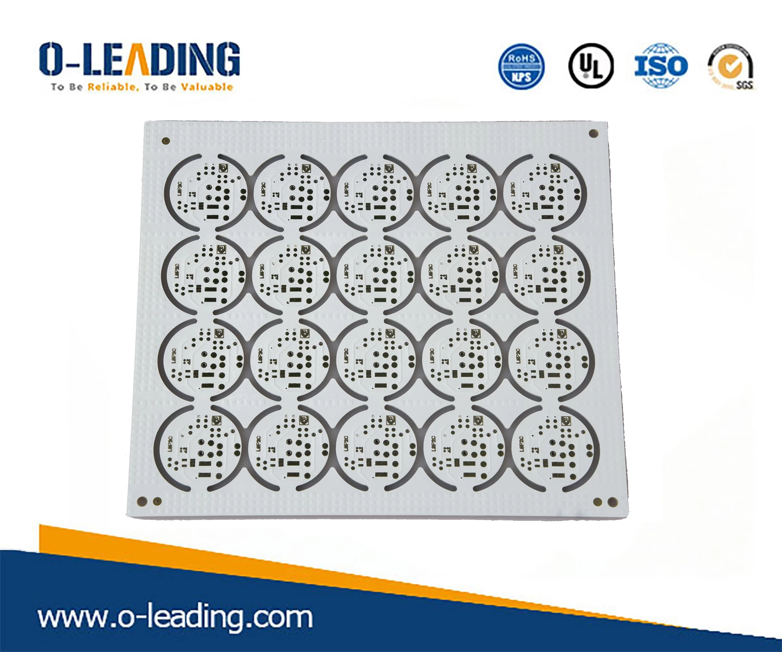
7. For the power line processing power line parasitic characteristics of the worst DC resistance and self-inductance, so we widen as much as possible when laying the power line.
8. The current on the input and output cables of the amplifier is very small, so the parasitic effects they are very susceptible to are very harmful to them.
9. For signal paths exceeding 1 CM, it is best to use a controlled impedance and a termination line (matching resistor).
10.Amplifier Driven Resistive Load In order to solve the stability problem, a common technique is to introduce a resistor ROUT and preferably close to the op amp. This uses a series output resistor to achieve isolation of the capacitive load.


