


Innovation is the driving force for sustainable development of the PCB industry
LED Lighting manufacturer china
The innovation of printed circuits, first of all, is the innovation of PCB products and markets. The noise-printed electronic circuits have brought revolutionary changes to PCB products and production processes.
Printed circuit boards are an indispensable accessory for modern electronic devices. Whether it is high-end electronic equipment, or household appliances and electronic toys, there are indispensable PCBs for loading electronic components and electrical signals. PCBs are followed by the entire electronic information industry. The development of the development.
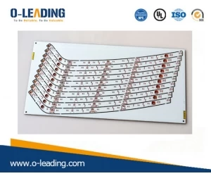
Innovations in printed circuits are first and foremost in innovation in PCB products and markets. The earliest PCB products were single-panel, with only one layer of conductor on the insulation board. The line width was measured in millimeters and was commercialized for use in semiconductor radios. In the future, with the advent of televisions, computers, etc., PCB products will be innovated, with double-sided and multi-layer boards. There are two or more layers of conductors on the insulating board, and the line width is gradually reduced. In order to adapt to the miniaturization and light weight development of electronic equipment, flexible PCB and rigid-flex PCB have emerged.
Single Side PCB manufacturer china
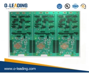
Nowadays, the main market of PCB is in the fields of computers, communication equipment, home electronics and automotive electronics. PCB products are mainly composed of multi-layer boards and high-density interconnection boards. With the development of high-speed and large-capacity computers, mobile phones to multi-functional intelligent, TVs to high-definition 3D, and automobiles to high-security, HDI printed boards have also changed from wire connection functions to electronic circuit functions. In addition to the basic conductor lines, PCB products also include passive components such as resistors and capacitors, and active components such as IC chips. The new generation of HDI printed boards is a buried component printed board containing components inside. A new generation of printed boards is suitable for high-frequency and high-speed signal transmission applications. The PCB layers will contain optical fibers and waveguides to form an optoelectronic printed board suitable for signal transmission above 40 GHz.
It is precisely because of the continuous innovation of PCB products that we are ushered in the spring of one development of printed circuits. Intelligent mobile phones will bring the climax of embedded component printed boards, LED energy-saving lighting will bring the climax of metal-based printed boards, and e-books and thin-film displays will bring the climax of flexible circuit boards. (Ultra-thin PCB manufacturer china )
The innovation of printed circuits is based on technological innovation. The traditional technology for PCB fabrication is copper foil etching, which uses a copper-clad insulating substrate to remove unwanted copper layers by chemical solution etching, leaving the required copper conductors to form a line pattern; for the double-sided and multi-layer boards The connection is made by drilling and electroplating copper. Nowadays, this traditional process has been difficult to adapt to the production of micro-scale fine-line HDI boards. It is difficult to achieve rapid and low-cost production, and it is difficult to achieve the goals of energy saving, green production, and only technological innovation can change this situation.
For the technological innovation of printed circuits, people have been pursuing semi-additive and additive techniques, that is, depositing copper layers on insulating substrates to form circuit patterns. This is an improvement on the traditional subtraction method. Energy consumption and high cost. The new road to innovation is printed electronic circuits that revolutionize PCB products and manufacturing processes. Printed electronic circuit technology uses a pure printing method to realize the electronic circuit pattern, that is, using screen printing or offset printing or inkjet printing process, the functional ink is printed on the insulating substrate to obtain the required electronic circuit. This technology can simplify production processes, save raw materials, reduce pollutants, and reduce production costs. If equipped with roll-type processing equipment, it can achieve high-volume, low-cost production.