


How can the PCB design meet EMC requirements as much as possible without causing too much cost press
The increased cost of PCBs due to EMC is usually due to the increase in the number of ground planes to enhance the shielding effect and the addition of ferrite bead, choke and other high-frequency harmonic suppression devices. In addition, it is usually necessary to match the shielding structure on other institutions to make the entire system pass the EMC requirements. The following provides only a few design techniques for PCBs to reduce the effects of electromagnetic radiation generated by the circuit.
Whenever possible, use slower signal slew rate components to reduce the high frequency components generated by the signal.
Pay attention to the location of high-frequency devices, not too close to the external connector.
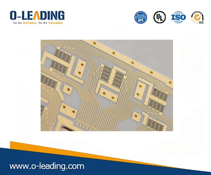
Pay attention to the impedance matching of high-speed signals, the routing layer and its return current path to reduce high-frequency reflection and radiation.
Power supply module manufacturer china
Place adequate decoupling capacitors on the power pins of each device to mitigate noise on the power and ground planes. Pay special attention to whether the frequency response and temperature characteristics of the capacitor meet the design requirements.
The ground near the external connector can be properly divided from the ground, and the ground of the connector should be connected to the chassis ground as close as possible.
Ground guard / shunt traces can be used appropriately next to some particularly high-speed signals. But pay attention to the effect of guard / shunt traces on the characteristic impedance of the trace.
The power plane is 20H smaller than the ground plane, where H is the distance between the power plane and the ground plane.