


How Are High Quality Printed Circuit Boards Made?
o-leading.com
o-leading.com
2017-12-28 15:33:23
Nearly all electronics products today contain printed circuit boards (PCBs). High quality printed circuit board manufacturing technology has allowed electronic items to become increasingly smaller and more complex; key to today’s dynamic and rapidly-progressing electronic innovations. While the PCB manufacturing process can vary, the main elements involved remain the same.
Here is a quick summary of the steps involved in the manufacture of high quality printed circuit boards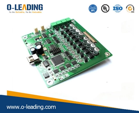
PCB Solutions adheres to a long-standing commitment of using only top-quality materials, in each of these important phases. Ensuring that the final output leaves nothing to chance.
After the foil surface of the substrate is degreased, the panels pass through a vacuum chamber where the bare printed circuit boards have a thin layer of photoresist material pressed onto the surface of the foil. The vacuum chamber keeps air bubbles from being trapped between the foil and the photoresist.
Quality assurance is key at this phase and not to be overlooked. At PCB Solutions we can’t imagine hiring an ‘cheap’ multilayer PCB manufacturer in china who does not adhere to such quality measures resulting in a final output that does not meet our strict standards.
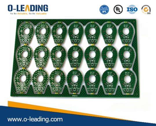
The printed circuit pattern mask is laid on top of the photoresist and the panels are exposed to ultraviolet light. Photoresist becomes more soluble when exposed to ultraviolet light and only those areas of the board where tracks are desired are covered in the resist. When the mask is removed, an alkaline developer is sprayed on to dissolve the irradiated photoresist in the printed circuit pattern and the copper foil is left exposed on the substrate.
Here is a quick summary of the steps involved in the manufacture of high quality printed circuit boards
.
Our experienced circuit board designers at PCB Solutions use industry-leading computer-aided design software to lay out the custom circuit pattern on the circuit board. The substrate most often used to manufacture printed circuit boards is a type of fiberglass-reinforced epoxy laminate known as FR4. (Flexible printed circuit boards use a flexible plastic such as polyamide.) The epoxy resin has a copper foil bonded to one or both sides. The copper is etched away from the substrate surface to create the desired pattern. China pcb manufacturers typically use an etching process employing the chemical ferric chloride.
Our experienced circuit board designers at PCB Solutions use industry-leading computer-aided design software to lay out the custom circuit pattern on the circuit board. The substrate most often used to manufacture printed circuit boards is a type of fiberglass-reinforced epoxy laminate known as FR4. (Flexible printed circuit boards use a flexible plastic such as polyamide.) The epoxy resin has a copper foil bonded to one or both sides. The copper is etched away from the substrate surface to create the desired pattern. China pcb manufacturers typically use an etching process employing the chemical ferric chloride.
PCB Solutions adheres to a long-standing commitment of using only top-quality materials, in each of these important phases. Ensuring that the final output leaves nothing to chance.
After the foil surface of the substrate is degreased, the panels pass through a vacuum chamber where the bare printed circuit boards have a thin layer of photoresist material pressed onto the surface of the foil. The vacuum chamber keeps air bubbles from being trapped between the foil and the photoresist.
Quality assurance is key at this phase and not to be overlooked. At PCB Solutions we can’t imagine hiring an ‘cheap’ multilayer PCB manufacturer in china who does not adhere to such quality measures resulting in a final output that does not meet our strict standards.
The printed circuit pattern mask is laid on top of the photoresist and the panels are exposed to ultraviolet light. Photoresist becomes more soluble when exposed to ultraviolet light and only those areas of the board where tracks are desired are covered in the resist. When the mask is removed, an alkaline developer is sprayed on to dissolve the irradiated photoresist in the printed circuit pattern and the copper foil is left exposed on the substrate.
That's all, thanks for reading!