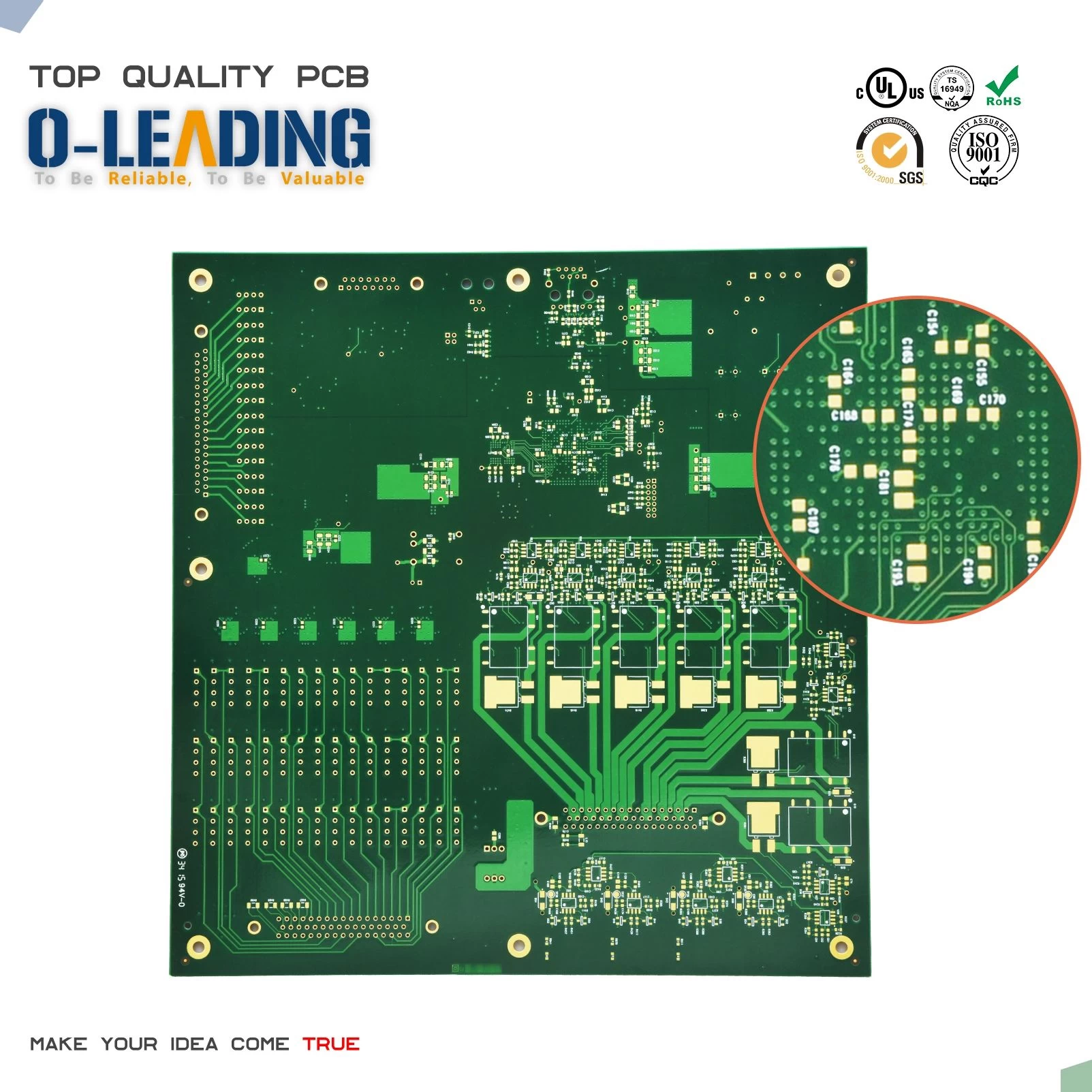
The principle of selecting the PCB and the grounding point of the enclosure
o-leading.com
o-leading.com
2017-09-27 20:38:58
What is the proper choice of the point of the PCB and the grounding of the enclosure?
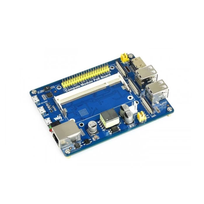
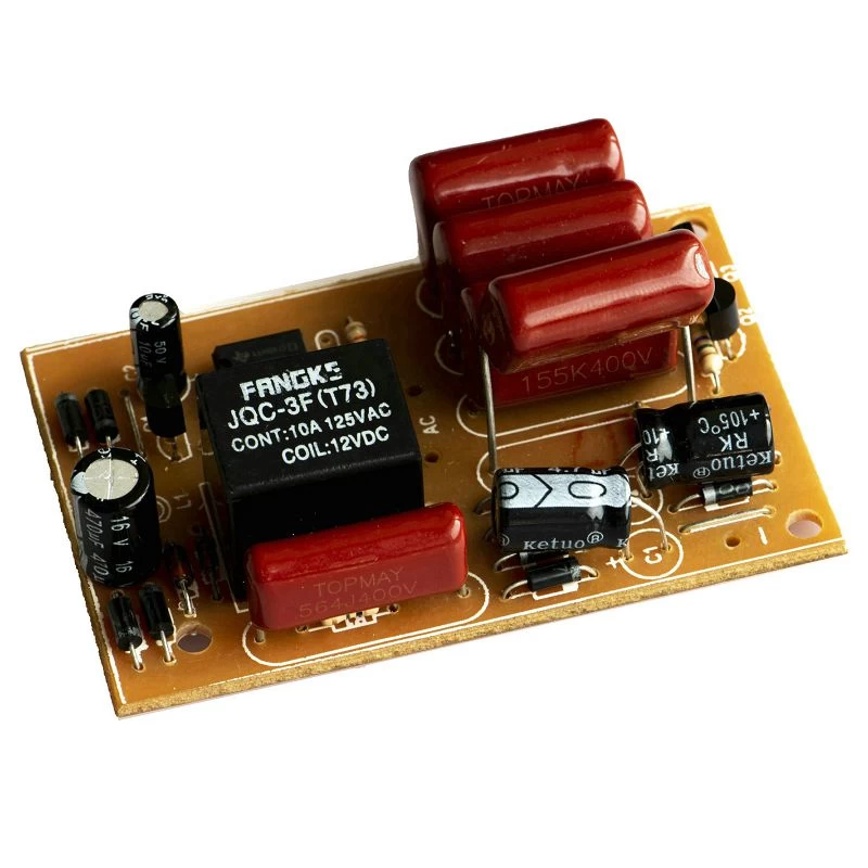
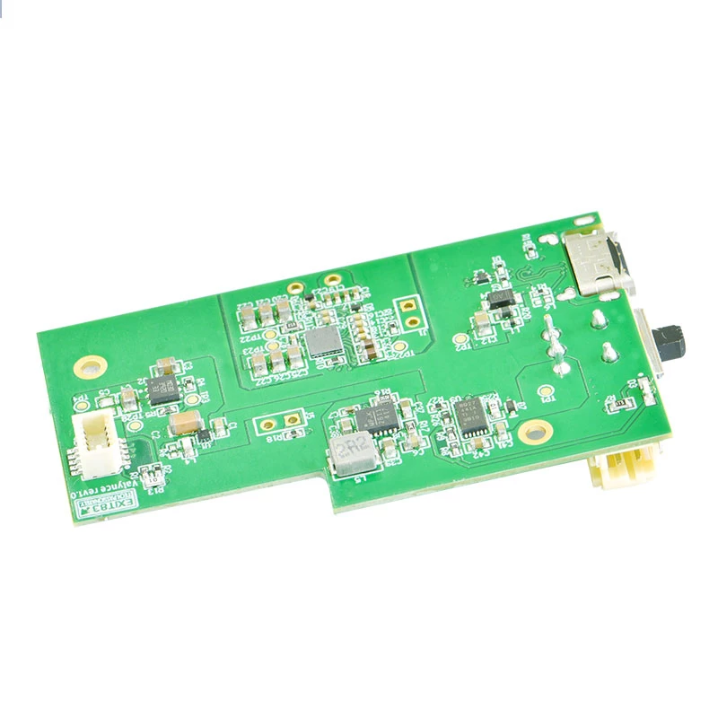
The principle of selecting the PCB and shell location is to use the chassis ground to provide a low impedance path to the return current (returning, current) and to control the path of this return current. For example, the PCB layer can be connected to the chassis ground by means of a fixed screw near the high-frequency device or the clock generator to minimize the area of the entire current loop and to minimize
The principle of selecting the PCB and shell location is to use the chassis ground to provide a low impedance path to the return current (returning, current) and to control the path of this return current. For example, the PCB layer can be connected to the chassis ground by means of a fixed screw near the high-frequency device or the clock generator to minimize the area of the entire current loop and to minimize
electromagnetic radiation.

How many aspects should the circuit board DEBUG start from?
As far as digital circuits are concerned, first of all, three things are determined in sequence:
As far as digital circuits are concerned, first of all, three things are determined in sequence:
1.. Make sure that all the power values are designed to meet the needs of the design. Some systems with multiple power supplies may require a certain order of speed and speed between certain power supplies.
2. make sure that all clock signal frequencies are normal and there is no non monotonic (non-monotonic) problem on the edge of the signal. 3. make sure the reset signal meets the specification requirements. These are normal, the chip should be issued the first cycle (cycle) signal. Next, follow the system operation principle and bus protocol to debug.

