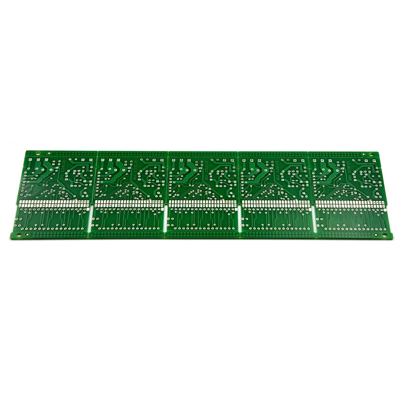
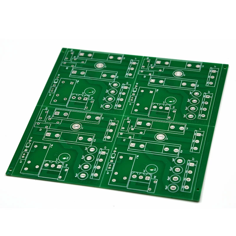
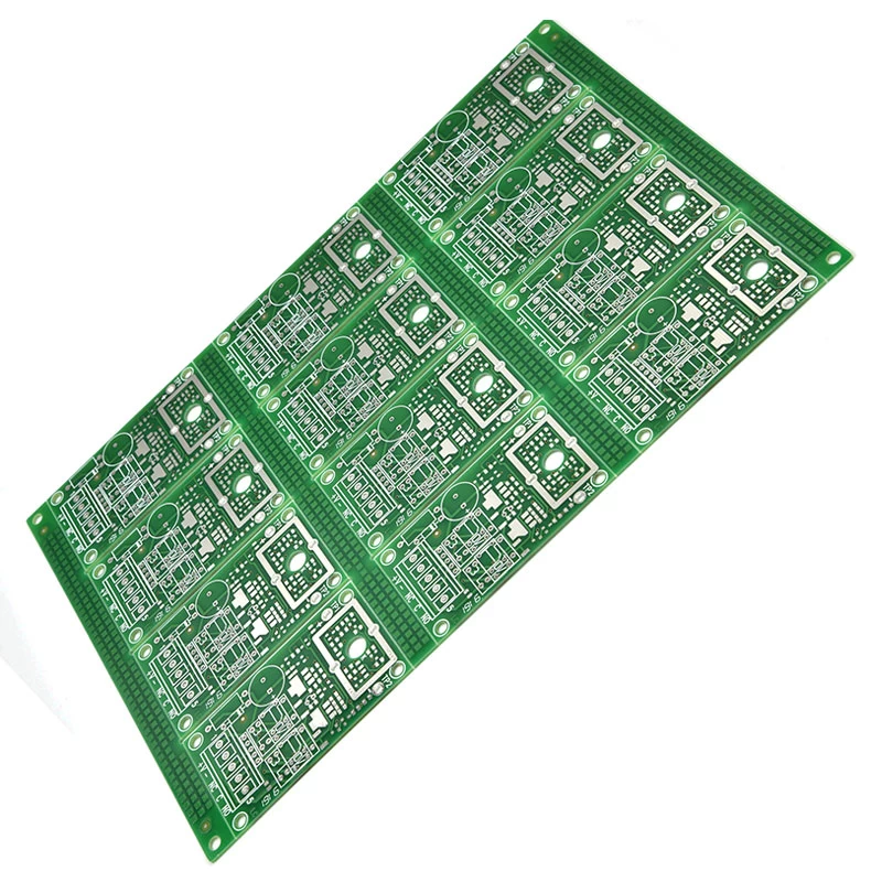
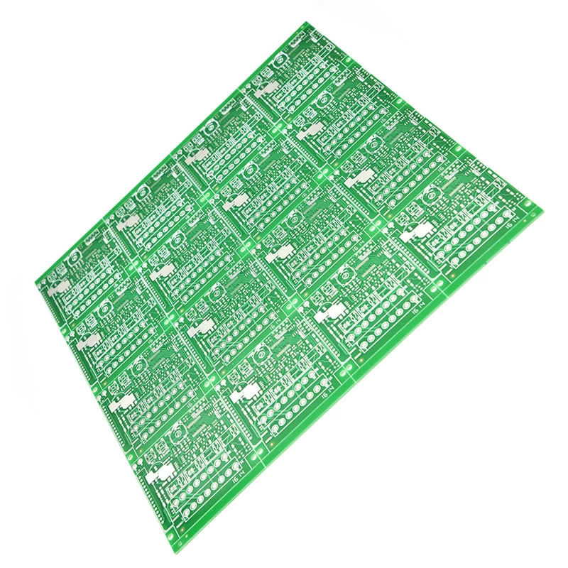
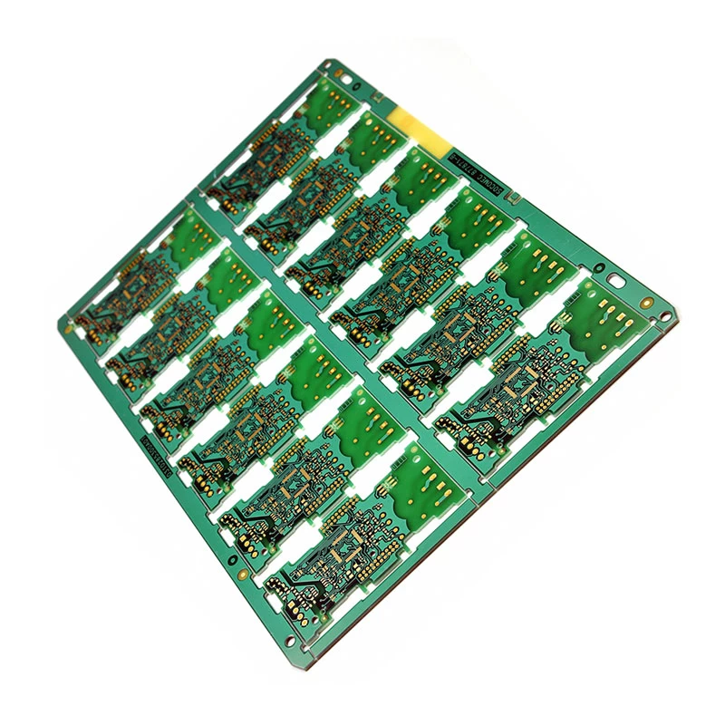
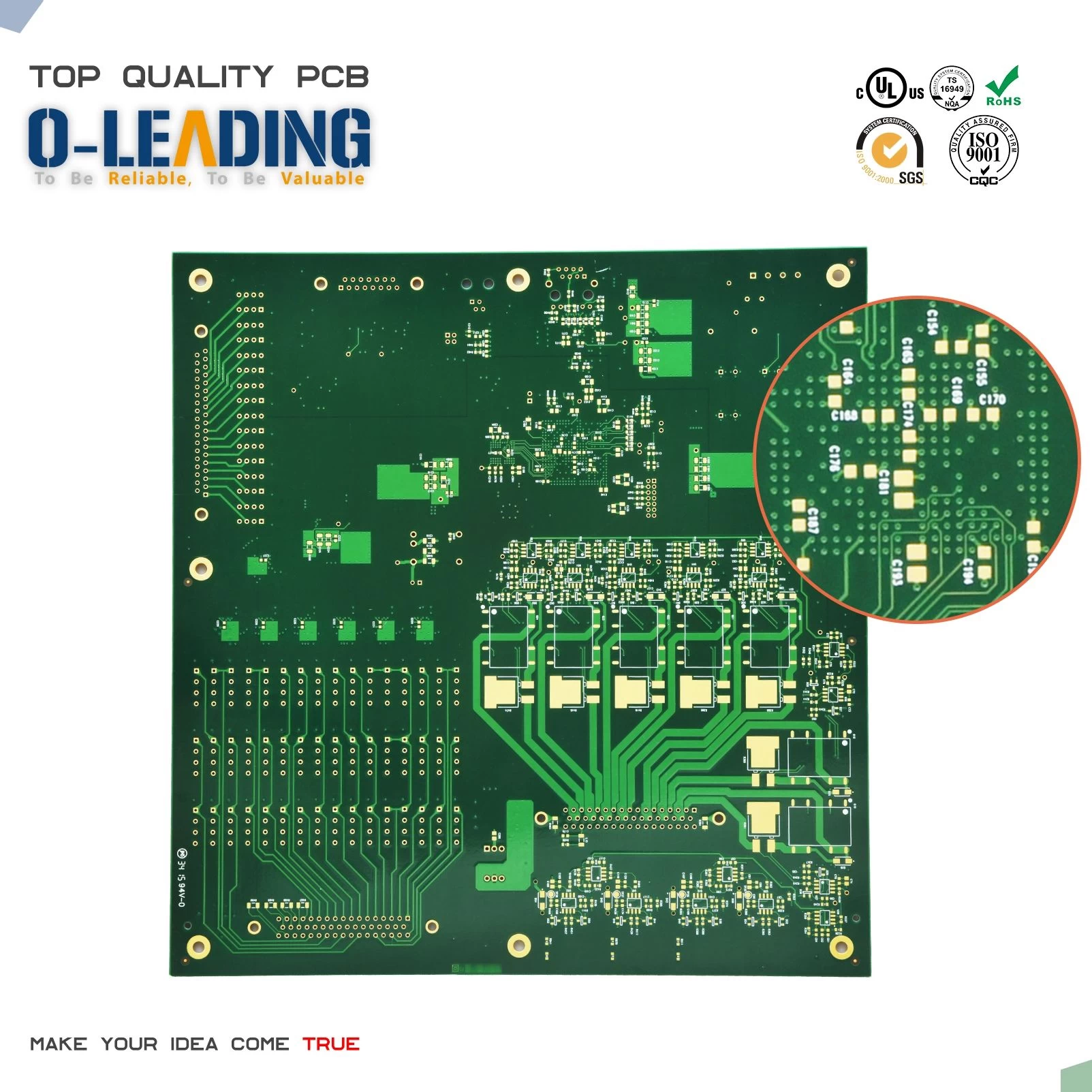
What should be noticed and what are the rules for PCB jigsaw?
PCB Jigsaw puzzle are things that PCB factories often do:
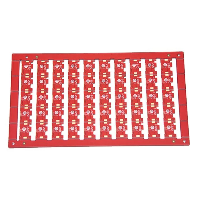
The first is the problem of Jigsaw puzzle,We know that the main problem of Jigsaw puzzle is to save production costs.For PCB panel width ≤260mm ~ 300mm, it varies according to different production lines. Because we may have a lot of materials, one processing gun of its own processing equipment corresponds to one module, so if the exceeds the range of the module, the processing speed will become very slow.
Halogen Free PCB manufacturer china

The outer frame (clamping edge) of the PCB puzzle should be carefully considered to ensure that the PCB puzzle will not be deformed after being fixed on the fixture (generally, V-grooves are not allowed on this side). Orientation should be consistent, and mirroring cannot occur, which will cause machining coordinate positioning problems.
Halogen Free manufacturer china
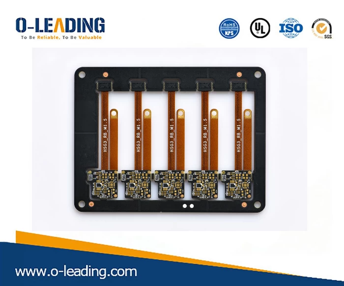
Secondly, there must be no connector protruding at the edges (between the outer frame of the puzzle board and the inner small board, and between the small board and the small board). If this situation exists, it will prevent the cutting of the tool after the welding is completed.
In order to ensure the position and level of the detection plate, we need to set more than three positioning points on the edge of the plate. Through optical detection of these three points, we can get the reference coordinates of the entire processing and the level of the plate.
The correct method is that the distance is 5mm from the edge and the direction of travel is different when the direction of travel is inconsistent (easy to distinguish the direction of entry): [When setting the reference positioning point, usually leave a 1.5mm larger solderless area around the positioning point. Similar pads or other similar]
Laser Stencil manufacturer china
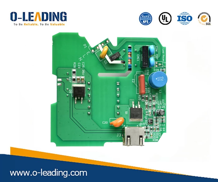
There must be at least three positioning holes in each small board, 3 ≤ hole diameter ≤ 6 mm, and wiring or patches are not allowed within 1 mm of edge positioning holes (to prevent misjudgment). PCB jigsaw is mainly to save production and processing costs (which will make the machine processing speed several times faster). Irrational design will be full of problems in the later stage. You can take a closer look to prevent problems.


