


Two functions of PCB board with large area copper: heat dissipation and anti-interference
Generally speaking, large-area copper-clad copper has two functions. One is to dissipate heat, and the power is increased due to excessive current of the circuit board. Therefore, in addition to adding necessary heat-dissipating components, such as heat sinks, cooling fans, etc., but for some circuit boards, It is still not enough. If it is just a simple heat dissipation, increase the area of the copper foil and increase the soldering layer, and add tin to enhance heat dissipation.
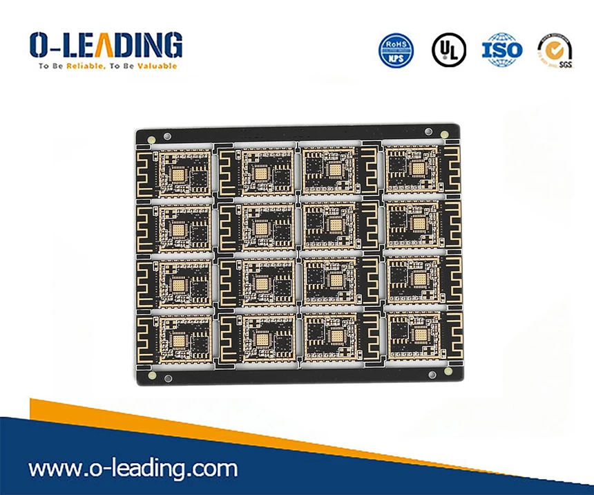
Rogers PCB factory china.
It is worth noting that due to the large area of copper, the over-peak or long-term heating of the PCB causes the adhesion between the PCB and the copper foil to be reduced. The volatile gas accumulated in the long-term can not be discharged, due to the thermal expansion and contraction. The copper foil is swollen and peeled off, so if the copper area is very large, consider whether there is such a problem, especially when the temperature is relatively high, it can be opened or designed into a grid.
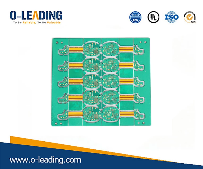
Teflon PCB factory china.
The other is to enhance the anti-interference ability of the circuit. Since large-area copper can reduce the impedance of the ground wire, the signal can be shielded to reduce mutual interference, especially for some high-speed PCB boards, except for the thickening of the ground line as much as possible. The vacant place should be grounded, that is, “full ground”, which can effectively reduce the parasitic inductance. At the same time, large-area grounding can effectively reduce noise radiation. For example, for some touch chip circuits, a ground wire is placed around each button to reduce the anti-interference ability.