


Tips for taking high-frequency and high-speed signal lines on the PCB side
According to Maxwell's electromagnetic field theory, a changing electric field produces a changing magnetic field in its surrounding space, and a changing magnetic field produces a changing electric field. Thus, the varying electric field and the changing magnetic field are interdependent, mutually excited, alternately generated, and propagated in space from near and far at a certain speed. This is electromagnetic radiation.
This has two diametrically opposite effects: on the positive side, all RF communications, wireless interconnects, and inductive applications benefit from the benefits of electromagnetic radiation; and the harmful side is that electromagnetic radiation causes crosstalk and electromagnetic compatibility. Aspects of the problem.
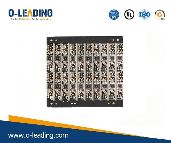
high-density PCB technology.
When the electromagnetic wave frequency is low, it can only be transmitted by the tangible electric conductor; when the frequency is gradually increased, the electromagnetic wave will overflow outside the conductor, and the medium can transmit energy without the medium.
This is a type of radiation. In low-frequency electrical oscillations, the mutual change between magnetoelectricity is relatively slow, and almost all of its energy is returned to the original circuit without energy radiation. However, in high-frequency electrical oscillations, the magnetoelectric interactions become very fast, and energy cannot be reversed back to the original oscillating circuit, so that the electrical energy and magnetic energy propagate into the space in the form of electromagnetic waves as the electric field and the magnetic field change periodically.
Laser Stencil manufacturer china.
According to the above theory, each section of the wire flowing through the high-frequency current will have electromagnetic radiation, and the radiation intensity is proportional to the frequency. Some wires on the PCB are used for signal transmission, such as DDR clock signals, LVDS differential signal transmission lines, etc., and it is not desirable to have too much electromagnetic radiation to lose energy and cause interference to other circuits in the system; and some wires are used as antennas. Like a PCB antenna, it is desirable to convert energy into electromagnetic waves as much as possible.
For high-speed signal transmission lines on PCBs (such as DDR clock signals, HDMI LVDS high-speed differential transmission lines), we always hope to reduce the radiation generated during signal transmission and reduce the electromagnetic radiation generated by signal transmission lines. Some design principles have been made. If the EMI of the signal transmission line is to be reduced, the distance between the signal transmission line and the reference plane constituting the signal return path should be as close as possible. If the ratio of the width W of the transmission line to the distance H of the reference plane is less than 1:3 , can significantly reduce the external radiation intensity of the microstrip transmission line.
For the microstrip transmission line, the wide and complete reference plane can also reduce the external radiation intensity of the electric field. The reference plane corresponding to the microstrip transmission line should be at least three times the width of the transmission line, and the wider the reference plane, the better.
If the reference plane is not sufficiently wide relative to the micro-single transmission line, the coupling of the electric field to the reference plane is small, and the external radiation of the electric field is significantly increased.