There are always a few places where the PCB design cannot be continuous. What should I do?
Characteristic impedance: Also known as "characteristic impedance", it is not a DC resistance and is a concept in long-line transmission. In the high frequency range, during the signal transmission process, a transient current is generated between the signal line and the reference plane (power or ground plane) due to the establishment of the electric field. LED Lighting manufacturer china.
If the transmission line is isotropic, as long as the signal is transmitting, there is always a current I, and if the output voltage of the signal is V, during the signal transmission, the transmission line is equivalent to a resistor, the size is V/I. This equivalent resistance is called the characteristic impedance Z of the transmission line.
During the transmission of a signal, if the characteristic impedance of the transmission path changes, the signal will be reflected at the node where the impedance is discontinuous.
Factors affecting the characteristic impedance are: dielectric constant, dielectric thickness, line width, and copper foil thickness.
EMBEDDED CAPACITANCE BOARD.
[1] Gradient line
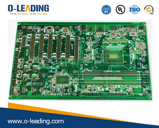
Some RF devices have smaller packages, SMD pad widths may be as small as 12 mils, and RF signal line widths may be more than 50 mils. A gradient line is used to disable line width abrupt changes. The gradient line is as shown in the figure, and the line of the transition part should not be too long.
NELCO N4000-13EP.
[2] corner
If the RF signal line is at a right angle, the effective line width at the corner will increase, and the impedance will be discontinuous, causing signal reflection. To reduce discontinuities, there are two ways to handle the corners: chamfers and fillets. The radius of the arc angle should be large enough. Generally speaking, it is guaranteed that R>3W. As shown on the right.
[3] Large pad
When there is a large pad on the 50-ohm microstrip line, the large pad is equivalent to the distributed capacitance, which destroys the characteristic impedance continuity of the microstrip line. Two methods can be improved at the same time: first, the microstrip line medium is thickened, and then the ground plane below the pad is hollowed out to reduce the distributed capacitance of the pad. As shown below.
[4] Via
A via is a metal cylinder that is plated outside the via between the top and bottom layers of the board. Signal vias connect the transmission lines on different layers. The via stub is the unused portion of the via. Via pads are ring-shaped pads that connect vias to the top or internal transmission lines. The isolation disk is an annular gap in each power or ground plane to prevent short circuits to the power and ground planes.

