


Specification for PCB circuit board design with PowerPCB
The pcb circuit board design process is divided into six steps: netlist input, rule setting, component layout, wiring, inspection, copying, and output.
1.Netlist input in PCB copy board
There are two methods for netlist input. One is to use PowerLogic's OLE PowerPCB Connection function, select Send Netlist, and apply OLE function to keep the schematic and PCB design drawings consistent at any time to minimize the possibility of errors. Another method is to load the netlist directly in PowerPCB, select File-> Import, and enter the netlist generated by the PCB design schematic.
2.pcb circuit board design software design rules set
If the PCB design rules are already set during the PCB design schematic design stage, there is no need to set these rules again, because when the netlist is entered, the design rules have been entered into PowerPCB with the netlist. If the design rules are modified, the schematic must be synchronized to ensure that the schematic is consistent with the PCB. In addition to the design rules and layer definitions, there are some rules that need to be set, such as Pad Stacks, which need to modify the size of standard vias. If the designer creates a new pad or via, be sure to add Layer 25.
3.Component layout in pcb circuit board design software
After the PCB design netlist is entered, all components will be placed at the zero point of the work area and overlapped. The next step is to separate these components and arrange them neatly according to some rules, that is, the component layout.
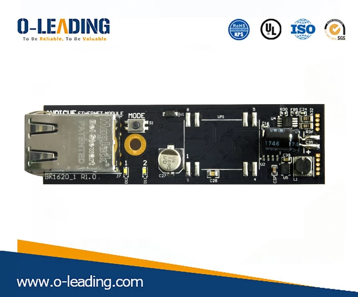
Lead free HASL wholesales china
4.PCB design and wiring
There are two kinds of PCB design wiring methods, manual wiring and automatic wiring. The manual routing function provided by PowerPCB is very powerful, including automatic pushing, online design rule checking (DRC), and automatic routing is performed by Specctra's wiring engine. Usually these two methods are used together. The common steps are manual-automatic-manual.
5.PCB copy board inspection
The pcb circuit board design inspection items include Clearance, Connectivity, High Speed, and Plane. These items can be selected by Tools-> Verify Design. If a high-speed rule is set, it must be checked, otherwise this item can be skipped. Checking for errors, you must modify the layout and routing.
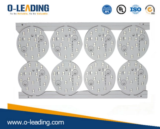
Lead free HAL wholesales china
6.pcb circuit board design review
PCB board design review according to "PCB checklist", including design rules, layer definition, line width, pitch, pads, via settings; also review the rationality of device layout, power, ground network routing , High-speed clock network routing and shielding, placement and connection of decoupling capacitors. If the PCB design review is unsuccessful, the PCB designer must modify the layout and wiring. After passing the review, the reviewer and the PCB designer sign separately.
7.pcb circuit board design output
The pcb circuit board design can be output to a printer or output light drawing files. The printer can print the PCB layer by layer, which is convenient for designers and reviewers to check. The light drawing files are handed to the board manufacturer to produce printed boards. The output of the light drawing file is very important, which is related to the success or failure of this design.