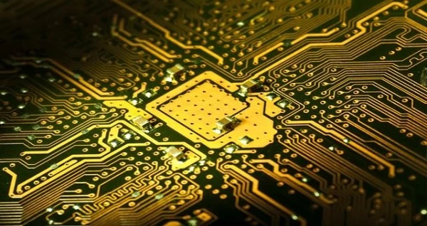
HDI pcb Printed circuit board is now widely used, maintenance problems also followed, when the PCB board problems, you will start to hurry to contact the circuit board manufacturers to deal with. Bad reason is very complicated, the following general for everyone on the basics.
First, the cause of the electronics factory caused by the bad: 1. Welding staff is an important part of the assembly section, and there is a certain technical requirements, if not in the course of the operation, there is a chance to cause PCBA bad tin; 2. Soldering iron soldering process is not stable; staff operation posture is not correct, did not choose the right soldering iron. 3. After welding the PCB board surface residual multi-board dirty, the main factors are no-clean flux is not appropriate; heating uneven or temperature is too low; tin furnace impurities, tin degree is too low; reasonable design; The
Second, PCB circuit board factory supply causes of the bad: 1. circuit board surface dirt caused by the residue attached to the pad can not be caused by tin. 2. The circuit board itself is reflected by the surface of the pad itself, resulting in a layer of pad surface oxide film, can not be on the flux, can not access to the PCB pad metal surface caused by bad tin. 3. Circuit board resistance welding quality is bad, coated with tin and then after the high temperature, there are ink off the phenomenon of ink particles stained with lead after the tin can not lead, poor quality.
Third, the special circumstances lead to the bad: 1. PCB circuit boards are required to vacuum packaging to the customer, and different surface treatment have a certain period of time, when the customer in the use of PCB board and opened the vacuum packaging, the remaining part of the product is useless End can not be vacuum packaging preservation time, may be used in the next time when the solder pad oxidation caused by bad tin. 2. OSP process circuit board in the open after the vacuum packaging, must be completed within 24 hours of the components, the other side of the components should also be completed within 48 hours patch, or prone to tin bad phenomenon or tin on the side of the other Not on the tin of the phenomenon. Because the OSP protective film will be volatile after the heat, when the first part of the paste when the parts, the protective film on the pad above the volatile, the other side bare copper exposed directly to the air, more than 12 hours is easy to copper surface oxidation.