


PCB layer design and electromagnetic compatibility have such a big relationship?
In the design process of high-speed circuit boards, electromagnetic compatibility design is an important and difficult point. This paper discusses how to reduce the propagation path of the coupling source and reduce the electromagnetic interference caused by the conduction coupling and radiation coupling, and improve the electromagnetic compatibility from the aspects of layer design and layer layout.
1 Introduction
Many reliability and stability problems of electronic products are caused by electromagnetic compatibility design. Common problems include signal distortion, excessive signal noise, unstable signals during work, the system is prone to crash, the system is susceptible to environmental interference, and poor anti-interference ability. Electromagnetic compatibility design is a fairly complex technology, with knowledge from design to electromagnetics. This article discusses some empirical techniques in terms of layer design and layer layout to provide some reference for electronic engineers.
2. Configuration of layers
The layers of the PCB board mainly include a power layer, a ground layer and a signal layer, and the number of layers is the sum of the number of each layer. In the design process, the first step is to coordinate and classify all sources and grounds, and various signals, and deploy and design on the basis of classification. In general, different power supplies should be divided into different layers, and different grounds should also have corresponding ground planes. Various special signals, such as clock high and frequency signals, need to be designed separately, and the ground plane needs to be added to shield the special signals to improve electromagnetic compatibility. When cost is also one of the factors to be considered, a balance must be found between the electromagnetic compatibility and cost of the system during the design process.

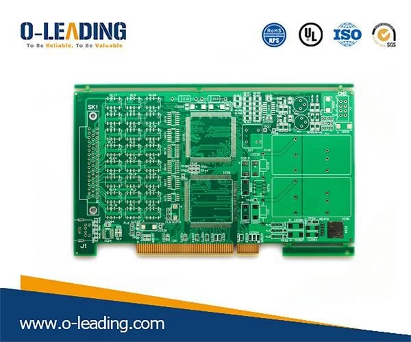
Multilayer board power supply module manufacturer china
The first consideration in the design of the power plane is the type and number of power supplies. If there is only one power supply, you can consider a single power layer. In the case of high power requirements, there can also be multiple power layers to power devices of different layers. If there are multiple power supplies, you can consider designing multiple power layers, or you can divide different power supplies on the same power layer. The premise of division is that there is no cross between power supplies. If there is a cross, multiple power supply layers must be designed.
The design of the number of signal layers should take into account the characteristics of all signals. The layering of special signals and shielding are issues to be considered in a limited way. In general, the design software is used for design, and then modified according to specific details. Signal density and the integrity of special signals must be issues that must be considered in layer design. For special information, the ground plane layer must be designed as a shield layer if necessary.
Under normal circumstances, if it is not purely cost considerations, it is not recommended to design single or double panels. Although the single panel and double panel have simple processing and low cost, but in the case of high signal density and complex signal structure, such as high-speed digital circuits or analog-to-digital hybrid circuits, because the single panel does not have a special reference ground layer, the loop The area increases and the radiation increases. Due to the lack of effective shielding, the anti-interference ability of the system is also reduced.
3. Layout design of PCB layer
After the signals and layers are determined, the layout of each layer also needs to be scientifically designed. The layout design of the middle layer of the PCB board design follows the following principles:
(1) The power plane is adjacent to the corresponding ground plane. The purpose of this design is to form a coupling capacitor and work with the decoupling capacitor on the PCB board to reduce the impedance of the power plane and obtain a wider filtering effect.
(2) The selection of the reference layer is very important. In theory, both the power layer and the ground plane can be used as the reference layer, but the ground plane can generally be grounded, so the shielding effect is much better than the power layer, so the ground plane is generally preferred. As a reference plane.
(3) The key signals of two adjacent layers cannot cross the partition. Otherwise, a larger signal loop will be formed, resulting in stronger radiation and coupling.
(4) To maintain the integrity of the ground plane, it is not possible to route on the ground plane. If the signal line density is too large, you can consider routing on the edge of the power layer.
(5) Design the ground layer below the key signals such as high-speed signals, pilot signals, and high-frequency signals, so that the signal loop path is the shortest and the radiation is minimal.
(6) In the process of high-speed circuit design, it is necessary to consider how to deal with the radiation of the power supply and the interference to the entire system. Generally, the area of the power plane should be smaller than the area of the ground plane, so that the ground plane can shield the power supply. Generally, the power plane is required to be indented twice as thick as the ground plane. If the indentation of the power layer is to be reduced, the thickness of the medium should be as small as possible.
Gold finger multilayer PCB suppliers
General principles to be followed in the layout design of multilayer printed boards:
(1) The plane of the power plane should be close to the ground plane and be designed below the ground plane.
(2) The wiring layer should be designed adjacent to the entire metal plane.
(3) The digital signal and the analog signal must have an isolated design. First of all, the digital signal and the analog signal must be avoided on the same layer. If it cannot be avoided, the analog signal and the digital signal can be routed in regions and the analog signal area can be slotted. Isolated from digital signal area. The same is true for analog power and digital power. Especially the digital power supply, the radiation is very large, it must be isolated and shielded.
(4) The printed lines in the middle layer form a planar waveguide, and the microstrip line is formed in the surface layer. The transmission characteristics of the two are different.
(5) Clock circuits and high-frequency circuits are the main sources of interference and radiation, and must be arranged separately and away from sensitive circuits.
(6) The stray currents and high-frequency radiated currents contained in different layers are different. When wiring, they cannot be treated equally.
4. Conclusion
Through the design of the number of layers and the layout of the layers can greatly improve the electromagnetic compatibility of the PCB board. Layer design should mainly consider the power layer and ground layer, high-frequency signals, special signals, and sensitive signals. The layout of the layer should mainly consider the layout of various couplings, ground and power lines, clock and high-speed signal layout, analog signal and digital information layout.