


PCB board ESD protection circuit design experience sharing
In the design of the PCB board, the anti-ESD design of the PCB can be realized by layering, proper layout and installation. In the design process, most of the design modifications can be limited to increasing or decreasing components through prediction. ESD can be well protected by adjusting the PCB layout. Here are some common precautions.
Recently, I have been doing ESD testing of electronic products. From the test results of different products, I found that this ESD is a very important test: if the board design is not good, when the static electricity is introduced, it will cause the product to crash or even the components. Damage. Previously only noticed that ESD would damage components, I did not expect that enough attention should be paid to electronic products.
ESD, also known as Electro-Static discharge. It is known from the learned knowledge that static electricity is a natural phenomenon, usually produced by contact, friction, and induction between electrical appliances. It is characterized by long-term accumulation and high voltage (which can generate static electricity of several thousand volts or even tens of thousands of volts). ), low power, low current and short duration of action. For electronic products, if the ESD design is not designed, it often causes unstable operation or even damage to electronic and electrical products.
Two methods are commonly used in ESD discharge testing: contact discharge and air discharge.
Contact discharge is the direct discharge of the device to be tested; air discharge is also called indirect discharge, which is the coupling of strong magnetic field to the adjacent current loop. The test voltage for these two tests is generally 2KV-8KV, which is different in different regions. Therefore, before designing, we must first understand the market targeted by the product.
The above two cases are basic tests for the human body when the electronic product is in contact with the electronic product due to human charging or other reasons. The chart below shows the air humidity statistics for some regions in different months of the year. It can be seen from the picture that Lasvegas has the least humidity throughout the year, and the electronics in the region should pay special attention to the protection of ESD.
Humidity varies from place to place around the world, but at the same time, in one area, if the air humidity is different, the static electricity generated will be different. The following table is the collected data, from which it can be seen that the static electricity becomes larger as the humidity of the air decreases. This also indirectly indicates the reason why the static spark generated when taking off the sweater is very large in the winter in the north.
"
Since static electricity is so harmful, how can we protect it? When performing electrostatic protection design, we usually take three steps: prevent external charge from flowing into the circuit board and cause damage; prevent external magnetic field from damaging the circuit board; and prevent the damage caused by the electrostatic field.
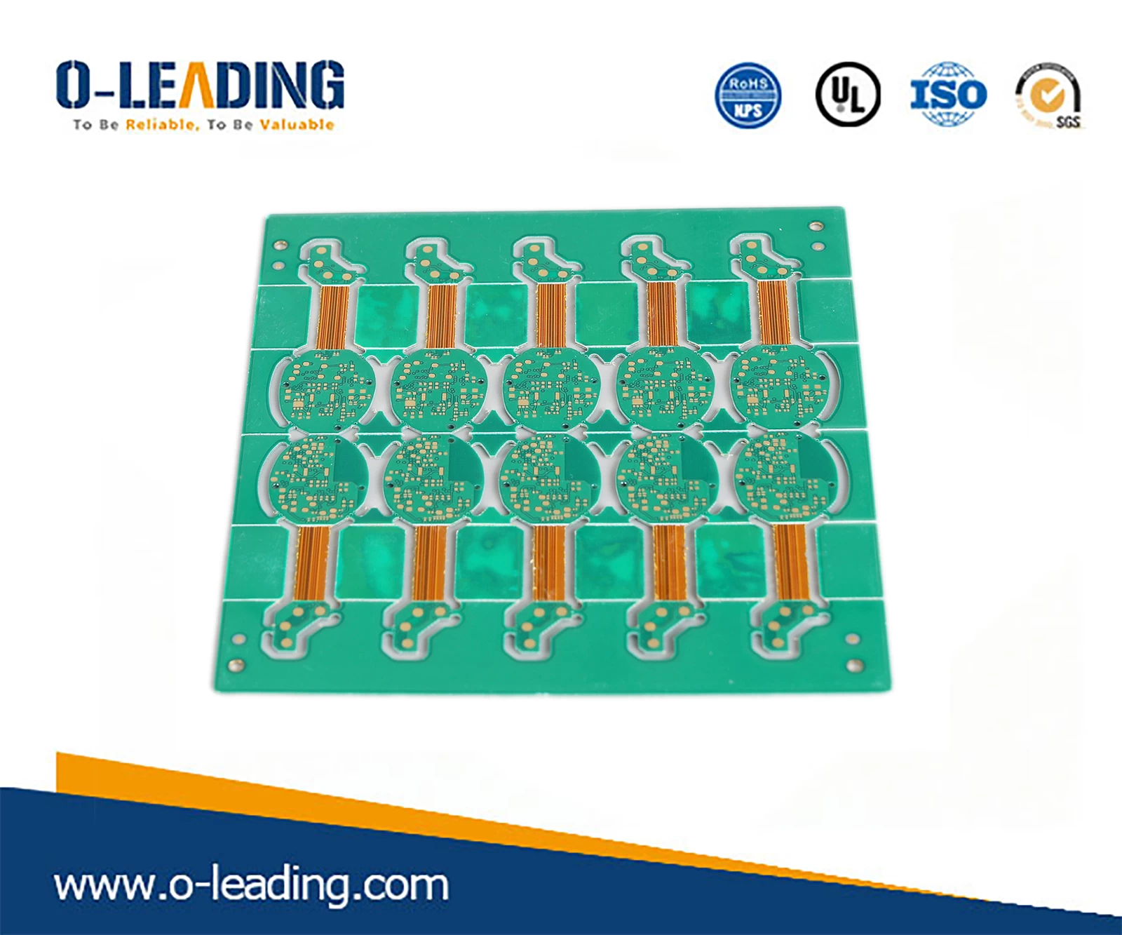
Printed circuit board manufacturer
In the actual circuit design, we will use one or several of the following methods for electrostatic protection:
1. Avalanche diode for electrostatic protection
This is also a method often used in design. A typical approach is to connect an avalanche diode to the ground in a critical signal line. The method utilizes the ability of avalanche diodes to respond quickly and has stable clamping, which can consume the accumulated high voltage in a short period of time to protect the board.
2, using high voltage capacitors for circuit protection
This method usually places a ceramic capacitor with a withstand voltage of at least 1.5KV at the position of the I/O connector or key signal, while the connection line is as short as possible to reduce the inductance of the connection line. If a capacitor with low withstand voltage is used, it will cause damage to the capacitor and lose its protection.
3, using ferrite beads for circuit protection
Ferrite beads can attenuate ESD current well and also suppress radiation. When faced with two problems, a ferrite bead will be a very good choice.
4, spark gap method
This method is seen in a material consisting of a layer of micro-belts made of copper, which is made up of triangular copper with pointed ends. The triangular copper is connected at one end to the signal line and the other is copper. Connected to the ground. When there is static electricity, a tip discharge is generated to consume electrical energy.
5, using the LC filter method to protect the circuit
The filter composed of LC can effectively reduce the high frequency static electricity entering the circuit. The inductive reactance of the inductor is very good at suppressing the high-frequency ESD from entering the circuit, and the capacitor shunts the high-frequency energy of the ESD to the ground. At the same time, this type of filter can also round the edge of the signal with a small RF effect, and the performance aspect has further improved in signal integrity.
6, multi-layer board for ESD protection
The choice of multi-layer boards is also a means of effectively preventing ESD when funds permit. In multi-layer boards, ESD is more quickly coupled to the low-impedance plane due to a complete ground plane close to the traces, thus protecting critical signals.
7. Method of protecting the periphery of the circuit board
This method usually draws traces around the board without a solder layer. Connect the trace to the enclosure as conditions permit, and note that the trace does not form a closed loop, which avoids the introduction of a loop antenna and introduces greater trouble.
8. Circuit protection using CMOS devices with clamp diodes or TTL devices
This method utilizes the principle of isolation for board protection. Because these devices are protected by clamp diodes, the design complexity is reduced in the actual circuit design.
9, more decoupling capacitors
These decoupling capacitors have low ESL and ESR values. For low frequency ESD, the decoupling capacitor reduces the loop area. Due to the ESL effect, the electrolyte is weakened, which can better filter out high frequency energy. .
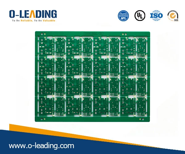
Aluminum base pcb factory china
In short, although ESD is terrible, it can even have serious consequences. However, only by protecting the power supply and signal lines on the circuit, it is possible to effectively prevent ESD current from flowing into the PCB. Among them, my boss often said that "a good grounding of a board is king." I hope this sentence can also bring you the effect of breaking the skylight.