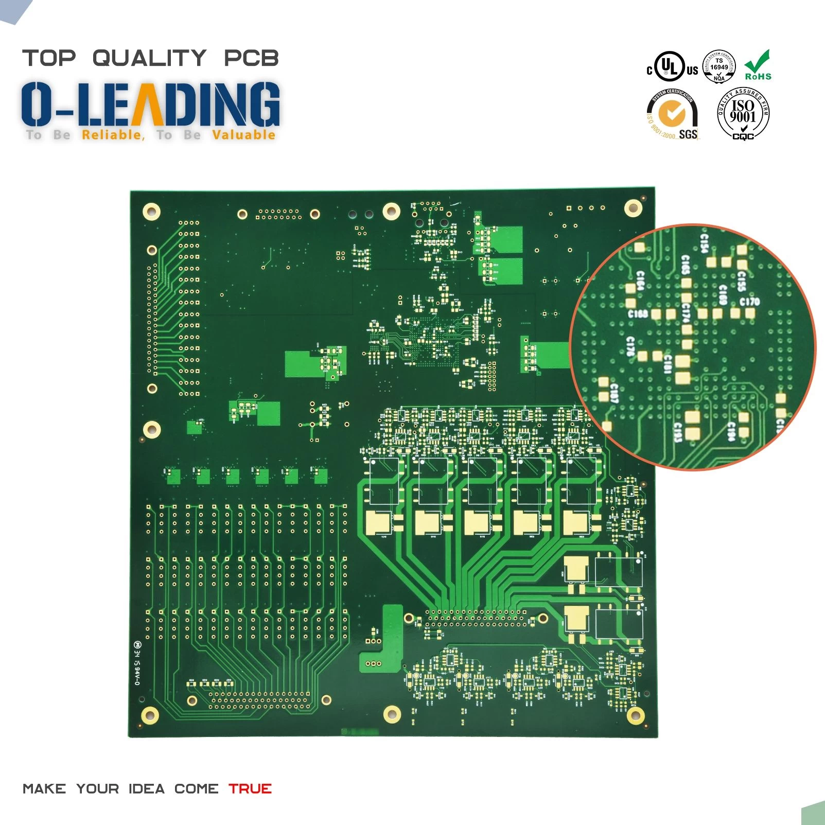
PCB and circuit anti-interference measures
The anti-interference problem is a very important link in modern circuit design. It directly reflects the performance and reliability of the entire system. For PCB engineers, anti-interference design is the focus and difficulty that everyone must master. The anti-interference design of the printed circuit board is closely related to the specific circuit. Next, we will only explain a few common measures for anti-interference design of the PCB.
1.Power cord design
According to the current of the printed circuit board, try to increase the width of the power line to reduce the loop resistance. At the same time, the direction of the power line and the ground line should be consistent with the direction of data transmission, which will help enhance the anti-noise capability.
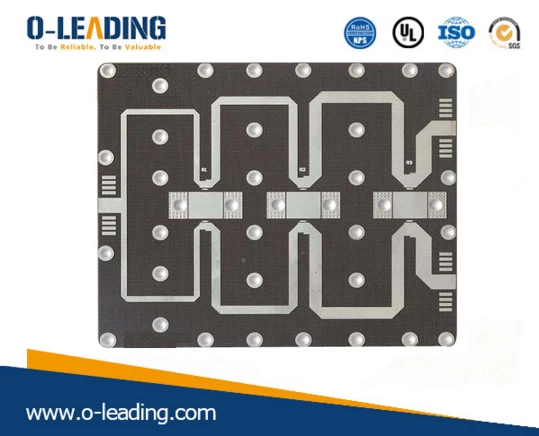
2.Ground design
The principles of ground wire design are:
(1) Digital ground is separated from analog ground. If there are both logic and linear circuits on the board, they should be separated as much as possible. The ground of low-frequency circuits should be grounded in a single point in parallel as much as possible. When the actual wiring is difficult, it can be partially connected in series and then grounded in parallel. High-frequency circuits should be grounded in multiple points in series. The ground wire should be short and leased. Use grid-like large-area ground foils around high-frequency components as much as possible.
(2) The grounding wire should be as thick as possible. If the ground wire is a very straight line, the ground potential changes with the change of current, which reduces the anti-noise performance. Therefore, the ground wire should be thickened so that it can pass three times the allowable current on the printed board. If possible, the ground wire should be above 2 ~ 3mm.
(3) The ground wire forms a closed loop. Most of the printed circuit board composed of digital circuits, the grounding circuit of the printed circuit can improve the anti-noise ability.
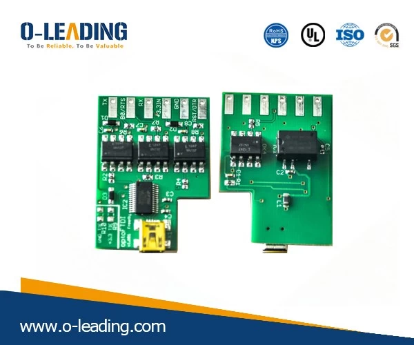
3.Relief capacitor configuration
One of the common practices of PCB design is to configure appropriate back-off capacitors in various key parts of the printed board.
The general configuration principles of the back-off capacitor are:
(1) The input end of the power supply is connected across an electrolytic capacitor of 10 ~ 100uf. If possible, it is better to connect above 100uF.
(2) In principle, each integrated circuit chip should be equipped with a 0.01pF ceramic capacitor. If the printed board has insufficient space, a 1 ~ 10pF capacitor can be arranged for every 4 ~ 8 chips.
(3) For devices with weak anti-noise ability and large power change during shutdown, such as RAM and ROM storage devices, a decoupling capacitor should be directly connected between the chip's power line and ground.
(4) The lead of the capacitor should not be too long, especially the high-frequency bypass capacitor should not have lead.
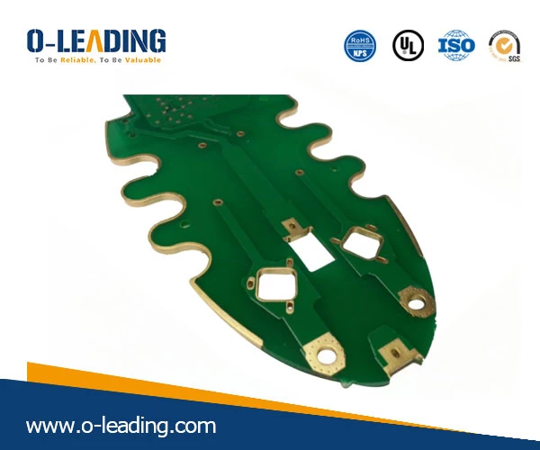
4.Methods for eliminating electromagnetic interference in PCB design
(1) Reducing loops: Each loop is equivalent to an antenna, so we need to minimize the number of loops, the area of the loop, and the antenna effect of the loop. Make sure that the signal has only one loop path at any two points, avoid artificial loops, and use the power plane as much as possible.
(2) Filtering: Filtering can be used to reduce EMI on power lines and signal lines. There are three methods: decoupling capacitors, EMI filters, and magnetic components.
Filter type
(3) Shielding.
(4) Minimize the speed of high-frequency devices.
(5) Increasing the dielectric constant of the PCB board can prevent high-frequency parts such as transmission lines near the board from radiating outward; increasing the thickness of the PCB board and minimizing the thickness of the microstrip line can prevent the overflow of the electromagnetic wires and prevent radiation.

