LED Circuit Board Has Good Heat Dissipation Function
o-leading.com
o-leading.com
2017-12-14 13:59:56
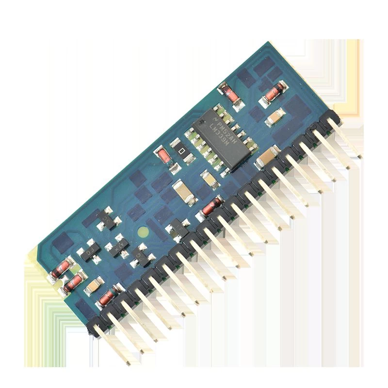
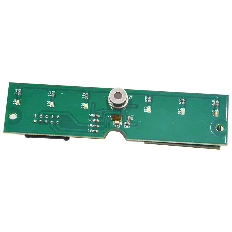
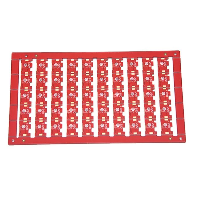
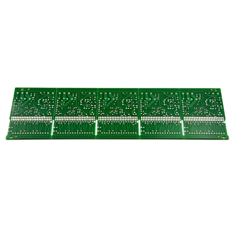
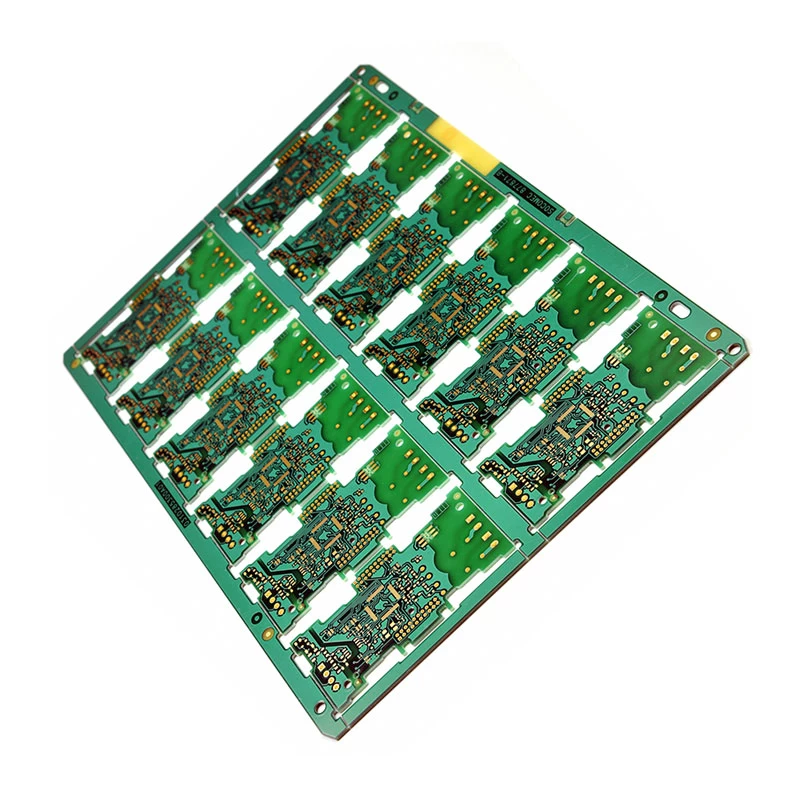
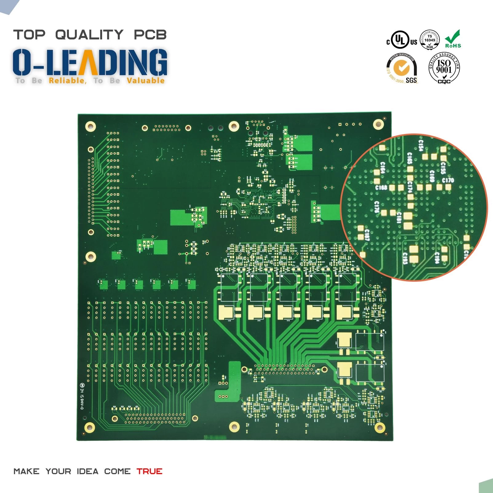
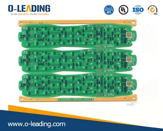
Led pcb board Printed circuit board has high-power led aluminum substrate, thick copper, ceramic board, Low-power led FR4 circuit board, High-temperature PCB. Because aluminum substrate has a good heat dissipation, high-power LED products are Aluminum substrates will be used.
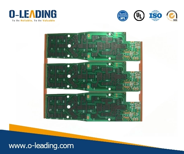
LED circuit boards are usually made of aluminum substrates and FR4 fiberglass panels. The most of the LED circuit boards are aluminum substrates because of the good heat dissipation. For example, LED fluorescent lamp circuit board with professional aluminum substrate to do, Mainly aluminum substrate can heat conduction fast, LED PCB is a good heat dissipation function of metal base CCL. And the general electronic circuit board is cardboard, fiberglass board, FR4.
The number of Watts high led most will choose aluminum substrate, LED PCB mainly heat dissipation is good. The low wattage of the LED lamp board is commonly used FR4 fiberglass board, LED PCB the number of low heat, with FR4 will be relative to the cost. but also to
Consider to use in that respect, save money, someone will use FR4, but considering the tile number is high, the heat dissipation is better, LED PCB also will select the aluminum substrate, this is uncertain, to combine with the actual request, according to circuit board file, some must use aluminum substrate.
The structure of the LED circuit board is a layer of insulating layer 6 (for example, made of a typical PI material), respectively, on both sides of the insulating layer (e.g. by means of bonding) line Layer 3, 7 (for example, the code Type of copper foil), on the outer side of the two-layer circuit layer respectively (such as bonding, coating, coating or printing) to play a protective role of the covering film layer 5, 5 (typically CVL). This existing technology The defect of the LED circuit board of the operation is manifold. For example, LED PCB the copper foil layer 3, 7 need to be bonded to the insulating layer 6 through, for example, the bonding process, and sometimes need to lay additional bonding layer, process steps The complex and additional bonding material will lead to an increase in the cost of the LED PCB finished product; Copper foil Layer 3, 7 of the line structure will be achieved by etching, LED PCB and copper foil layer 3, 7 of the interlayer conduction needs electroplating Mode plating through hole to achieve, it will inevitably bring pollution to the environment, and its energy consumption is high; Copper foil Layer 3, 7 and insulating layer 6, covering film layer 5, 5 adhesion to the position will inevitably affect the line Process steps for opening windows of the road plate and/or insulating layer and/or covering film layer to further increase the complexity of the manufacturing process and may affect the final reliability of the product due to its alignment process.
And then affect the product yield and actual working life. Not only that, because the copper foil layer 3, 7 exposure to air oxidation, resulting in solder joints (or solder plate) oxidation and lead to welding electronic components such as LED failure or even failure, LED PCB so in the existing technology of the copper foil layer 3, 7 is usually attached to cover the film, and also need to PCB copper foil layer 3, 7 of the exposed solder joints for passivation treatment , this not only makes the manufacturing process complex, but also increases costs. Therefore, the field needs a new circuit board which can simplify the process, LED PCB it can cancel the passivation process and improve the welding Reliability. In addition, copper foil Layer 3, 7 due to the use of copper production, high cost, so the field also need to be able to use other cheaper metal materials to make line layer, including solder tray To reduce the cost of the LED PCB material. Therefore, in this field, it is urgent to need a new technology simpler, cheaper led circuit board to reduce or even avoid the defects, Jane Production process and product structure, reduce costs, LED PCB reduce environmental pollution and energy consumption, improve product reliability and actual working life.
The structure of the PI layer sandwiched between two layers of copper in the LED circuit board product is omitted directly, and it is replaced by a simple non-copper foil layer containing nickel metal monolayer to act as a line layer, thus simplifying the fabrication process and product knot Structure, greatly reduces the material cost and the process cost, reduces the environmental pollution and the energy consumption, enhances the product the welding reliability and the actual working life, and may increase the working current of the LED circuit board by led pcb board manufacturer.
On the other hand, an LED circuit board is disclosed, including a line layer made directly from a single layer of nickel-containing metal, and covering the front and back sides of the line layer, respectively.
Resistance models include one or more of 0603, 0805, and 0812. On the other hand, the invention discloses a method for making the LED circuit board, which includes providing a nickel-containing metal monolayer; The first punching or cutting of the nickel-containing metal sheet is formed and the line layer is arranged, and the reverse cover film is pressed on the back of the line layer and the second punching is carried out on the line layer.
or cutting, forming PCB assembly Printed circuit board, LED PCB and the front of the prototype circuit board affixed to the front cover the film and press.

LED circuit boards are usually made of aluminum substrates and FR4 fiberglass panels. The most of the LED circuit boards are aluminum substrates because of the good heat dissipation. For example, LED fluorescent lamp circuit board with professional aluminum substrate to do, Mainly aluminum substrate can heat conduction fast, LED PCB is a good heat dissipation function of metal base CCL. And the general electronic circuit board is cardboard, fiberglass board, FR4.
The number of Watts high led most will choose aluminum substrate, LED PCB mainly heat dissipation is good. The low wattage of the LED lamp board is commonly used FR4 fiberglass board, LED PCB the number of low heat, with FR4 will be relative to the cost. but also to
Consider to use in that respect, save money, someone will use FR4, but considering the tile number is high, the heat dissipation is better, LED PCB also will select the aluminum substrate, this is uncertain, to combine with the actual request, according to circuit board file, some must use aluminum substrate.
The structure of the LED circuit board is a layer of insulating layer 6 (for example, made of a typical PI material), respectively, on both sides of the insulating layer (e.g. by means of bonding) line Layer 3, 7 (for example, the code Type of copper foil), on the outer side of the two-layer circuit layer respectively (such as bonding, coating, coating or printing) to play a protective role of the covering film layer 5, 5 (typically CVL). This existing technology The defect of the LED circuit board of the operation is manifold. For example, LED PCB the copper foil layer 3, 7 need to be bonded to the insulating layer 6 through, for example, the bonding process, and sometimes need to lay additional bonding layer, process steps The complex and additional bonding material will lead to an increase in the cost of the LED PCB finished product; Copper foil Layer 3, 7 of the line structure will be achieved by etching, LED PCB and copper foil layer 3, 7 of the interlayer conduction needs electroplating Mode plating through hole to achieve, it will inevitably bring pollution to the environment, and its energy consumption is high; Copper foil Layer 3, 7 and insulating layer 6, covering film layer 5, 5 adhesion to the position will inevitably affect the line Process steps for opening windows of the road plate and/or insulating layer and/or covering film layer to further increase the complexity of the manufacturing process and may affect the final reliability of the product due to its alignment process.
And then affect the product yield and actual working life. Not only that, because the copper foil layer 3, 7 exposure to air oxidation, resulting in solder joints (or solder plate) oxidation and lead to welding electronic components such as LED failure or even failure, LED PCB so in the existing technology of the copper foil layer 3, 7 is usually attached to cover the film, and also need to PCB copper foil layer 3, 7 of the exposed solder joints for passivation treatment , this not only makes the manufacturing process complex, but also increases costs. Therefore, the field needs a new circuit board which can simplify the process, LED PCB it can cancel the passivation process and improve the welding Reliability. In addition, copper foil Layer 3, 7 due to the use of copper production, high cost, so the field also need to be able to use other cheaper metal materials to make line layer, including solder tray To reduce the cost of the LED PCB material. Therefore, in this field, it is urgent to need a new technology simpler, cheaper led circuit board to reduce or even avoid the defects, Jane Production process and product structure, reduce costs, LED PCB reduce environmental pollution and energy consumption, improve product reliability and actual working life.
The structure of the PI layer sandwiched between two layers of copper in the LED circuit board product is omitted directly, and it is replaced by a simple non-copper foil layer containing nickel metal monolayer to act as a line layer, thus simplifying the fabrication process and product knot Structure, greatly reduces the material cost and the process cost, reduces the environmental pollution and the energy consumption, enhances the product the welding reliability and the actual working life, and may increase the working current of the LED circuit board by led pcb board manufacturer.

On the other hand, an LED circuit board is disclosed, including a line layer made directly from a single layer of nickel-containing metal, and covering the front and back sides of the line layer, respectively.
Membrane。 According to an optimal embodiment of the utility model, LED PCB the nickel-containing metal line layer directly replaces the two-layer or multi-layer structure of the existing LED circuit board base material. According to another optimal embodiment of the utility model , the nickel-containing metal is a nickel-plated aluminum or nickel-plated aluminum alloy. According to another optimal embodiment of the utility model, LED PCB the nickel-containing metal is a nickel-plated iron or a nickel-plated ferroalloy. According to the utility model Another preferred embodiment of the line layer is a line layer formed by punching, cutting, or etching the nickel-containing metal monolayer. According to another optimal embodiment of the utility model, LED PCB the line layer package The solder plate containing the passivation. According to another optimal embodiment of the utility model, the thickness of the line layer is more than 3 ounces, preferably 6 ounces or greater than 6 disk divisions. According to another optimization of the utility model The line layer is a line layer formed directly by punching or cutting the nickel-containing metal monolayer. According to another optimal embodiment of the utility model, the LED circuit board is a flexible PCB (FPC). According to another optimal embodiment of the utility model, the nickel-containing metal is aluminum with a nickel laminated layer or an aluminum alloy with a nickel laminated layer. According to another optimal embodiment of the utility model , LED PCB the type of LED on the LED board of the utility model includes one or more of 335, 3528, 5050 and 5060, which can be installed on the LED circuit board of the utility model.
Resistance models include one or more of 0603, 0805, and 0812. On the other hand, the invention discloses a method for making the LED circuit board, which includes providing a nickel-containing metal monolayer; The first punching or cutting of the nickel-containing metal sheet is formed and the line layer is arranged, and the reverse cover film is pressed on the back of the line layer and the second punching is carried out on the line layer.
or cutting, forming PCB assembly Printed circuit board, LED PCB and the front of the prototype circuit board affixed to the front cover the film and press.

