How to deal with PCB crosstalk
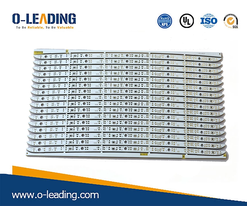
The development of electronic products is moving toward a small volume and high speed. The reduction in volume will lead to an increase in the layout and wiring density of the circuit, while the frequency of the signal is increasing, resulting in high crosstalk. Crosstalk is a problem that must be taken seriously in the design and production of PCBs.
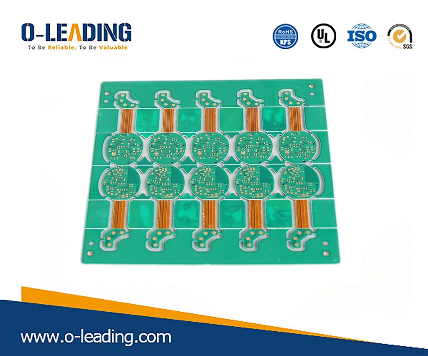
So, what should we pay attention to when designing the PCB?
1. The spacing between the lines should be as large as possible, because the larger the spacing, the smaller the influence between the capacitors and the smaller the electromagnetic field coupling.
2. The smaller the distance between the transmission line and the reference plane, the better, which will make it more tightly coupled and reduce the interference of adjacent lines.
3. If there are interferences in the signals of different layers, then the two lines are oriented perpendicular to each other. Because the lines are perpendicular to each other, the electric field and the magnetic field are perpendicular to each other, which can reduce the crosstalk between each other.
Double Side PCB manufacturer china.

4. Use a laminated dielectric material with the lowest dielectric constant whenever possible, which minimizes the thickness of the dielectric between the signal path and the return path given a characteristic impedance.
5. If protective wiring is used, try to reach the required width and use a via to short the guard wire to the return path.
6. If the signal changes the reference plane, the reference plane should be as close as possible to the signal plane.


