Blanking of printed circuit board PCB
o-leading.com
o-leading.com
2017-09-06 19:22:11
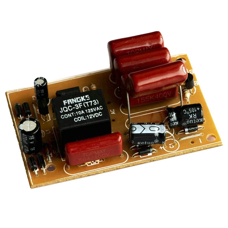
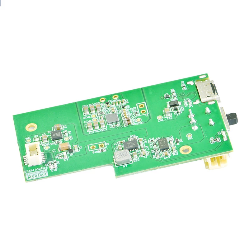
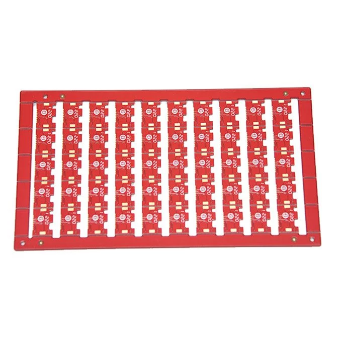
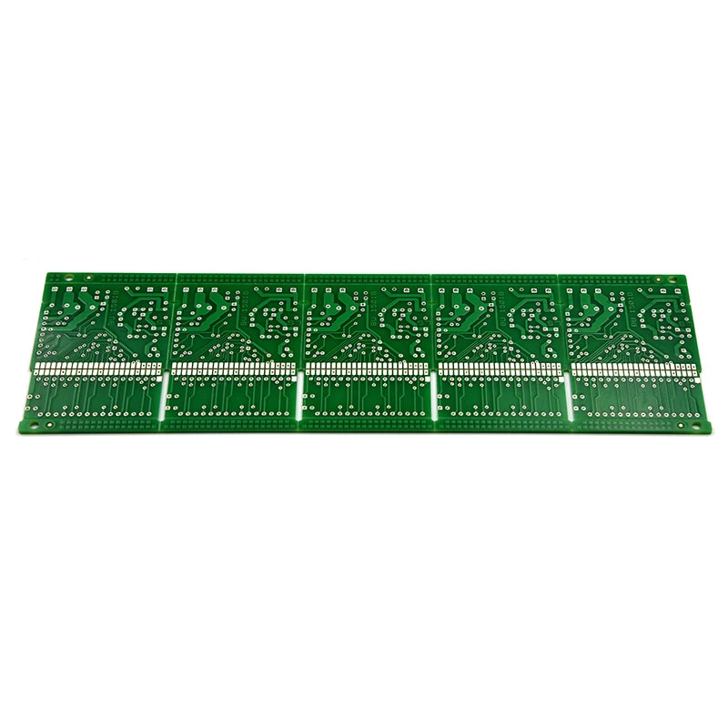
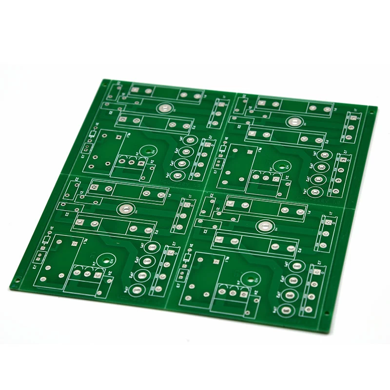
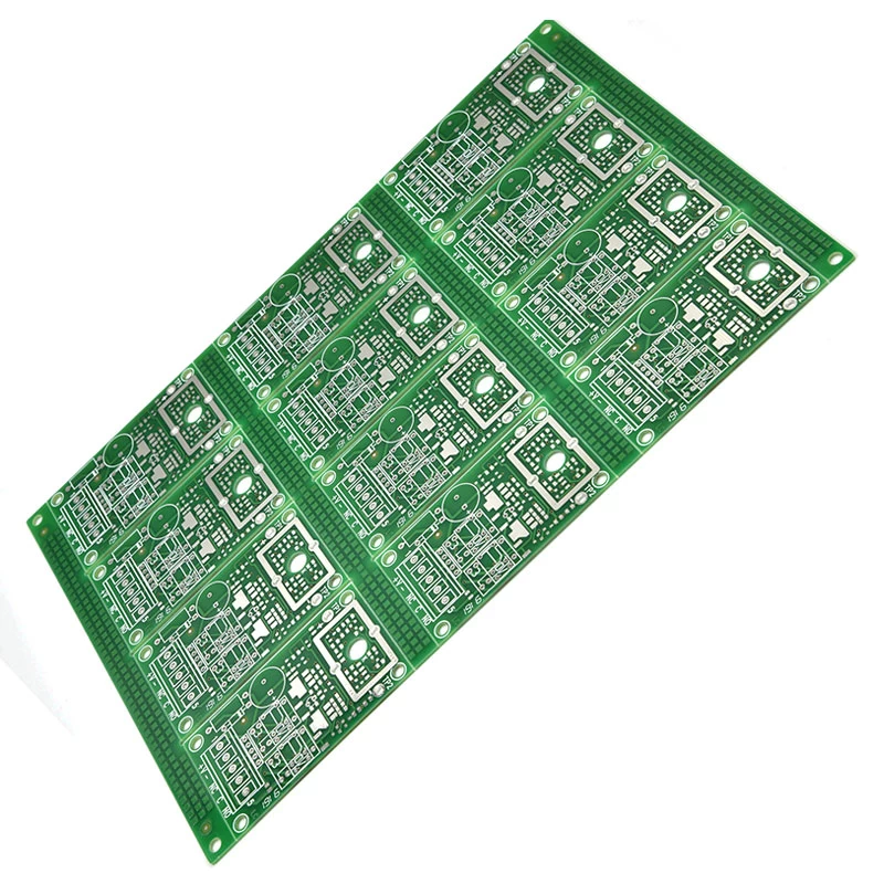
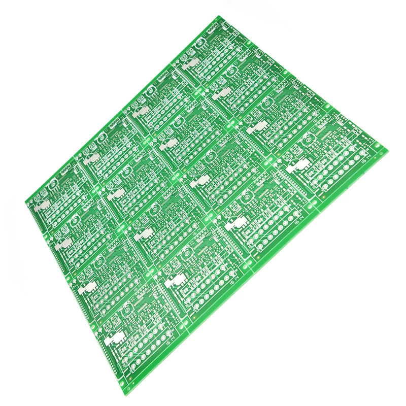
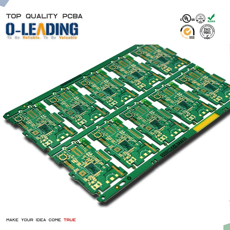
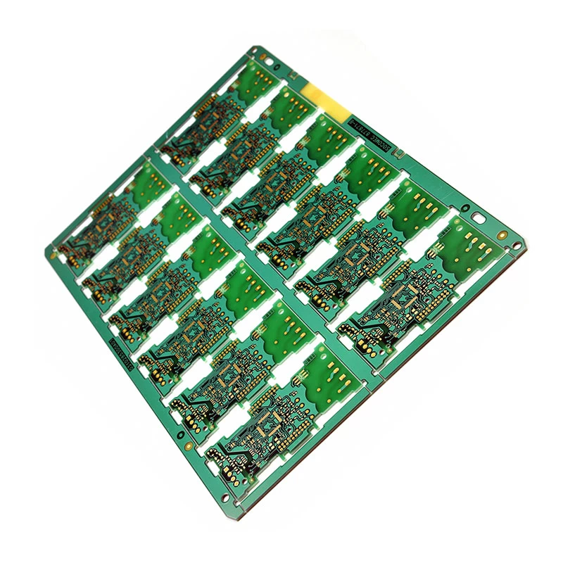
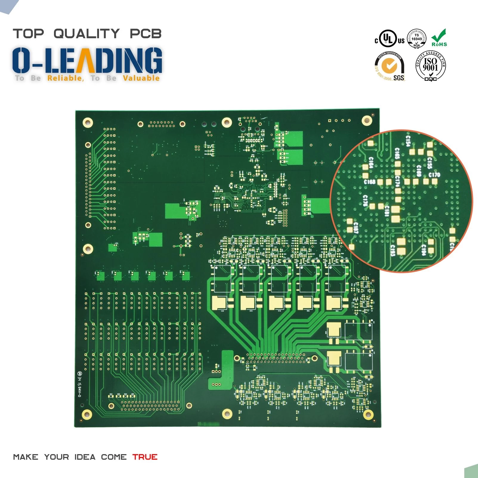
The blanking of the printed board, the hole and the shape processing can be carried out by the die cutting method. For the simple PCB or the PCB (High Quality PCBs china) which is not very high, punching method can be adopted. Suitable for low level and high-volume requirements, not very high PCB and shape requirements are not very high PCB production, and its lower cost.
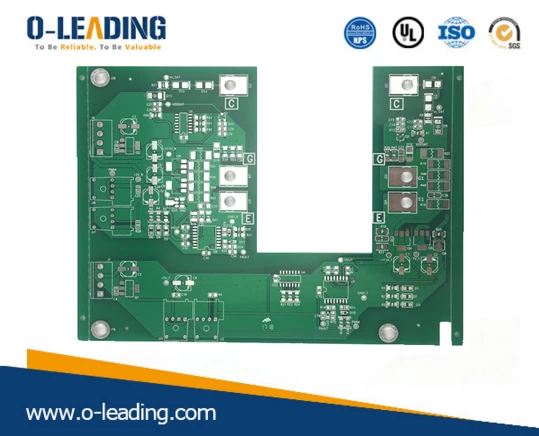
Punching: the production of large quantities of holes and types of large and complex shapes of single-sided paper substrates and double-sided non-metallic holes of epoxy glass cloth substrate, usually with a pay or a few die punching.
Contour processing: the production of large, single and double sided panels on printed boards, usually by die stamping. According to the size of the printed board, it can be divided into the upper blanking die and the falling die.
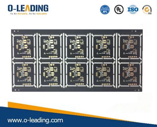
Compound processing: the hole and hole of the printed circuit board require high precision between the hole and the shape. At the same time, in order to shorten the manufacturing cycle and increase the productivity, the compound die is used to process the hole and shape of the single panel at the same time. Printed circuit board with the mould, the key is to mold design, processing, the need for professional and technical knowledge, in addition, the installation and debugging of the mold is also very important, at present most of the PCB mold production plant by processing factory.

Punching: the production of large quantities of holes and types of large and complex shapes of single-sided paper substrates and double-sided non-metallic holes of epoxy glass cloth substrate, usually with a pay or a few die punching.
Contour processing: the production of large, single and double sided panels on printed boards, usually by die stamping. According to the size of the printed board, it can be divided into the upper blanking die and the falling die.

Compound processing: the hole and hole of the printed circuit board require high precision between the hole and the shape. At the same time, in order to shorten the manufacturing cycle and increase the productivity, the compound die is used to process the hole and shape of the single panel at the same time. Printed circuit board with the mould, the key is to mold design, processing, the need for professional and technical knowledge, in addition, the installation and debugging of the mold is also very important, at present most of the PCB mold production plant by processing factory.

