


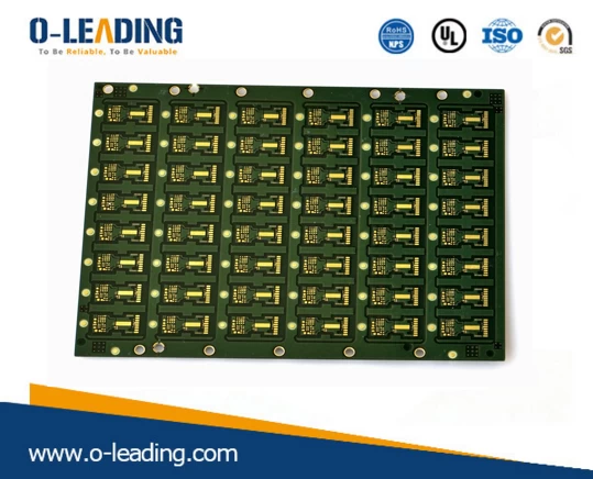
Heat resistance of HDI plate
o-leading.com
o-leading.com
2017-11-24 15:17:06
The heat resistance of HDI board is an important item in the reliable performance of HDI. The thickness of HDI board becomes thinner and thinner, and the requirement of its heat resistance is higher and higher. With the advancement of lead-free process, the requirement of heat resistance of HDI board is improved, and because the HDI plate is different from the ordinary multilayer through hole HDI pcb Printed circuit board in the layer structure, the heat resistance of HDI plate is different from that of the ordinary multilayer through hole PCB plate.
Heat resistance refers to the ability of PCB to resist thermal mechanical stress during welding. The mechanism of delamination in heat resistance test of PCB generally includes the following:
(1) when testing different materials in the sample, when the temperature changes, the high precision manufacturers of the circuit board have different expansion and contraction performance, and produce internal thermal mechanical stress in the sample, resulting in cracks and delamination.
(2) to test the micro defects (including voids, microcracks, etc.) in the sample, which is the stress concentration of the thermo mechanical and plays the role of stress amplifier. Under the stress of the sample, it is more likely to lead to cracks or delamination.
(3) volatile substances test samples (including volatile organic ingredients and water), multi-layer circuit board manufacturers in high temperature and extreme temperature changes, the rapid expansion of internal steam pressure, when the steam pressure reaches the expansion of micro defects test samples (including internal voids, micro cracks, etc.) will amplifier small defects the corresponding causes delamination.
Quick turn pcb Printed circuit board is prone to below the outer surface of the copper, which is due to the mounting and welding, PCB heat, volatile substances (including volatile organic ingredients and water) the rapid expansion of the outer surface of the copper barrier volatile substances (including volatile organic ingredients and water) to escape, resulting in internal steam pressure great, when the steam pressure expansion test samples within the reach of small defects (including voids, micro cracks, etc.) will correspond to the amplifier defects lead to delamination.