Do you know in the pcb design encountered these problems to be resolved?
o-leading.com
o-leading.com
2017-11-03 16:52:08
In the chip when the choice also need to consider the chip itself esd problem?
Whether it is double or multi-layer board, should be as much as possible to increase the area. In the choice of chips to consider the chip's own ESD characteristics, which are generally mentioned in the chip description, and even if different manufacturers of the same chip performance will be different. Design more attention, consider the overall point, make the performance of the circuit board will be a certain guarantee. But the ESD problem is still possible, so the protection of the organization is also important for ESD protection.
When doing pcb board, in order to reduce the interference, whether the ground should form a closed and form?
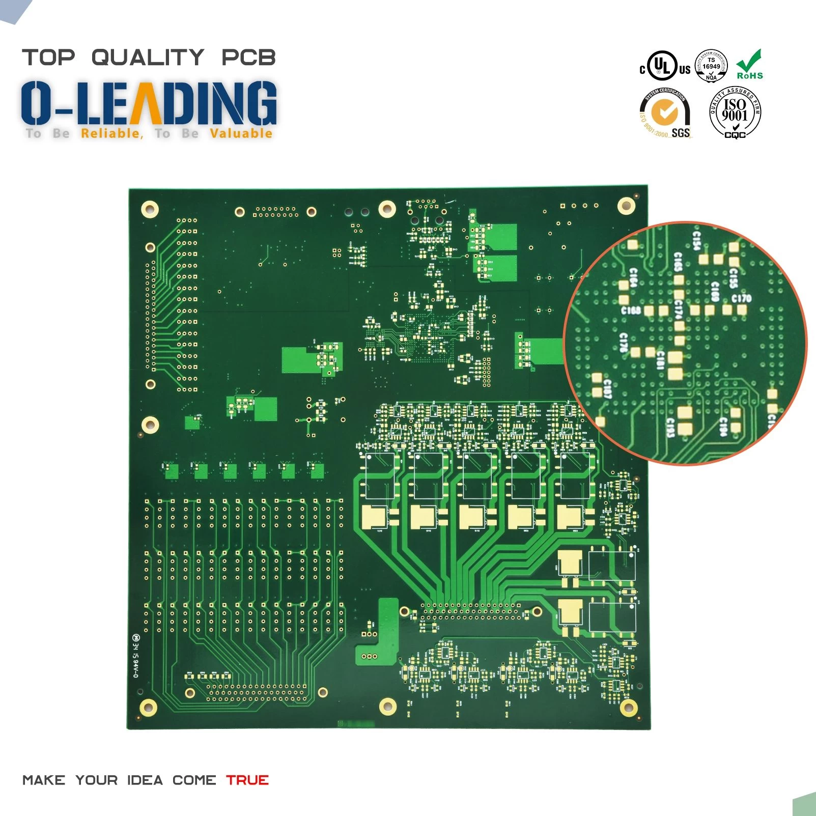
When doing PCB board, in general, have to reduce the area of the circuit in order to reduce the interference, when the cloth line, it should not be laid into a closed form, but cloth into a dendritic shape is good, there is as much as possible by The area of the earth.
If the simulator with a power supply, pcb board with a power supply, the two power supply ground should be linked together?
If you can use a separate power supply is better, because such a power supply is not easy to produce interference, but most of the equipment is a specific requirement. Since the simulator and PCB board with two power supply, according to my idea is not the total of its.
Whether it is double or multi-layer board, should be as much as possible to increase the area. In the choice of chips to consider the chip's own ESD characteristics, which are generally mentioned in the chip description, and even if different manufacturers of the same chip performance will be different. Design more attention, consider the overall point, make the performance of the circuit board will be a certain guarantee. But the ESD problem is still possible, so the protection of the organization is also important for ESD protection.

When doing pcb board, in order to reduce the interference, whether the ground should form a closed and form?
When doing PCB board, in general, have to reduce the area of the circuit in order to reduce the interference, when the cloth line, it should not be laid into a closed form, but cloth into a dendritic shape is good, there is as much as possible by The area of the earth.

If the simulator with a power supply, pcb board with a power supply, the two power supply ground should be linked together?
If you can use a separate power supply is better, because such a power supply is not easy to produce interference, but most of the equipment is a specific requirement. Since the simulator and PCB board with two power supply, according to my idea is not the total of its.

