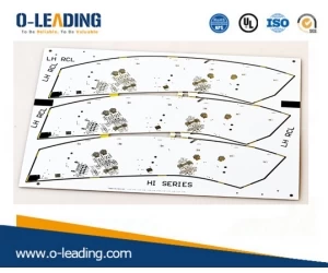
Balance the PCB design method
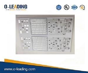
Ultra-thin PCB manufacturer china
Balanced structures avoid bending
The best reason to design a PCB without an odd layer is that the odd layer is easy to bend. When the PCB is cooled after the multilayer circuit bonding process, the PCB will be bent due to different lamination tension during the cooling of the nuclear structure and foil-applied structure. As the thickness of the circuit board increases, the risk of bending the composite PCB with two different structures increases. The key to eliminating the circuit board bend is to use balanced lamination. Although a degree of bent PCB meets the specification requirements, subsequent processing efficiency will be reduced, resulting in increased costs. Because special equipment and process are required during assembly, component placement accuracy is reduced, which will damage quality.
Use even layer PCB
When there are odd layers of PCB in the design, balance lamination can be achieved by using the following methods to reduce PCB production cost and avoid PCB bending. The following methods are arranged in order of preference.
1. A signal layer and use it. This method can be used if the power supply layer of the PCB is even and the signal layer is odd. The added layer does not increase cost, but it can shorten delivery time and improve PCB quality.
2. Add an additional power layer. This method can be used if the power supply layer of the PCB is odd and the signal layer is even. An easy way is to add a layer between layers without changing other Settings. The remaining layers are marked by duplicating the layers in the middle. This is the same as the electrical properties of foils in a thickened formation.
3. Add a blank signal layer near the center of the PCB stack. This approach minimizes cascading imbalance and improves PCB quality. Press the odd number of layers for wiring, and then add a blank signal layer to mark the remaining layers. In microwave circuit and mixed medium (medium has different dielectric constant) the circuit is adopted.
Advantages of balanced laminated PCB: low cost, no bending, short delivery time, quality assurance.
Please click here for more information: Impedance PCB manufacturer china

