


Avoid electromagnetic problems in PCB design (1)
1. Ground the PCB
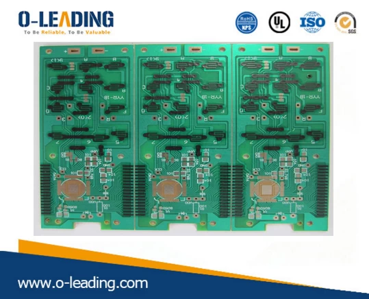
An important way to reduce EMI is to design the PCB ground plane. The first step is to make the ground area in the total area of the PCB circuit board as large as possible, which can reduce emissions, crosstalk and noise. Special care must be taken when connecting each component to a ground point or ground plane. Failure to do so will not take advantage of the neutralization effect of a reliable ground plane.A particularly complex PCB design has several stable voltages. Ideally, each reference voltage has its own ground plane. However, if there are too many ground layers, it will increase the manufacturing cost of the PCB and make the price too high. The compromise is to use separate ground planes at three to five different locations, each of which can contain multiple ground Single sided pcb on sale,OEM Ceramic substrate,OEM Double sided pcbplanes. This not only controls the manufacturing cost of the circuit board, but also reduces EMI and EMC.
If you want to minimize EMC, a low impedance grounding system is important. In a multilayer PCB, it is best to have a reliable ground plane instead of a copper thieving or scattered ground plane because it has a low impedance and provides a current path. .The length of time the signal returns to the ground is also important. The time for the signal to travel to and from the signal source must be equal, otherwise an antenna-like phenomenon will occur, making the radiated energy a part of EMI. Similarly, the traces that carry current to / from the signal source should be as short as possible. If the lengths of the source and return paths are not equal, ground bounce will occur, which will also cause EMI. Signals entering and exiting the signal source are not synchronized in time, which will cause antenna-like phenomena, which will radiate energy and cause EMI.
2. Distinguish EMI
Because of different EMI, a good EMC design rule is to separate analog and digital circuits. Analog circuits with high amperage or high current should be kept away from high-speed traces or switching signals. If possible, protect them with a ground signal. On a multilayer PCB, the analog traces should be routed on one ground plane, while the switch traces or high-speed traces should be routed on another ground plane. Therefore, signals with different characteristics are separated.
A low-pass filter can sometimes be used to eliminate high-frequency noise coupled to surrounding traces. The filter suppresses noise and returns a stable current. It is important to separate the ground planes for analog and digital signals. Because of the unique characteristics of analog and digital circuits, it is important to separate them. Digital signals should have digital ground, and analog signals should terminate at analog ground.In digital circuit design, experienced PCB layout and design engineers pay special attention to high-speed signals and clocks. At high speeds, signals and clocks should be as short as possible and close to the ground plane, because as mentioned earlier, the ground plane keeps crosstalk, noise, and radiation within a manageable range. Digital signals should also be kept away from the power plane. If the distance is close, noise or induction can occur, weakening the signal.