Avoid electromagnetic problems in PCB design (2)
Crosstalk and traces are key
Traces are especially important to ensure the proper flow of current. If the current comes from an oscillator or other similar device, it is especially important to keep the current separate from the ground plane or not to run it in parallel with another trace. Two parallel high-speed signals can generate EMC and EMI, especially crosstalk. The resistance path must be minimized and the return current path must be as short as possible. The length of the return path trace should be the same as the length of the transmit trace.
For EMI, one is called the "aggressive trace" and the other is the "victimized trace." Inductive and capacitive coupling can affect “victimized” traces due to the presence of electromagnetic fields, which can cause forward and reverse currents on the “victimized traces”. In this way, ripples are generated in a stable environment where the transmitted and received lengths of the signal are almost equal.
In a well-balanced, stable trace environment, the induced currents should cancel each other out to eliminate crosstalk. However, we are in an imperfect world, and such things will not happen. Therefore, our goal is to keep crosstalk on all traces to a minimum. If the width between parallel lines is doubled, the effect of crosstalk can be minimized. For example, if the trace width is 5 mils, the minimum distance between two parallel traces should be 10 mils or more.
As new materials and new components continue to emerge, PCB designers must continue to address electromagnetic compatibility and interference issues.
Decoupling capacitor
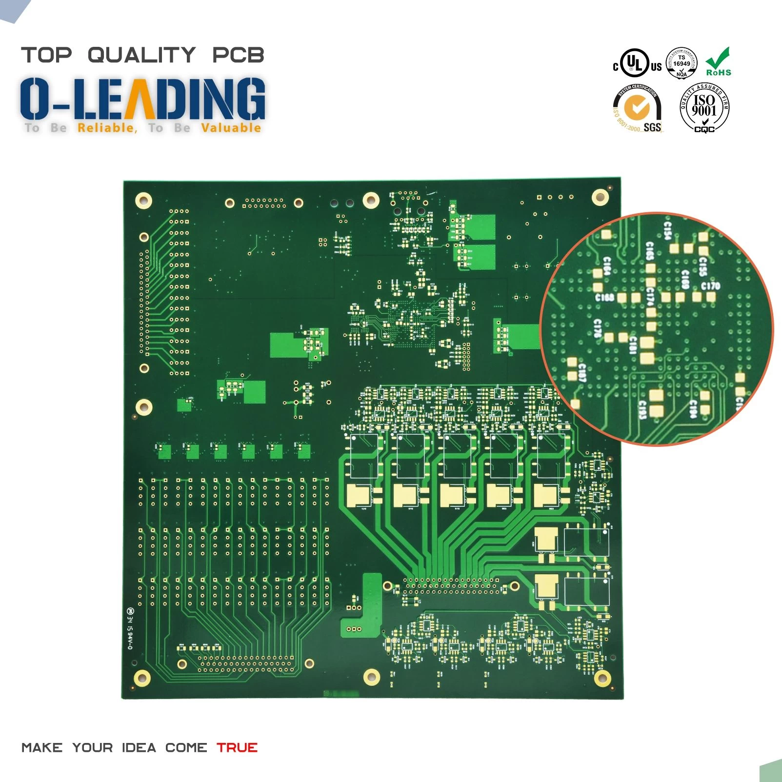
Decoupling capacitors can reduce the adverse effects of crosstalk. They should be located between the power and ground pins of the device to ensure low AC impedance and reduce noise and crosstalk. To achieve low impedance over a wide frequency range, multiple decoupling capacitors should be used.
Use of decoupling capacitors around the ball grid array reduces crosstalk.An important principle for placing decoupling capacitors is that the capacitor with the smallest capacitance value should be as close to the device as possible to reduce the influence of inductance on the traces. This particular capacitor is placed as close as possible to the device's power pins or power traces, and the capacitor's pad is connected directly to the via or ground plane. If the traces are long, use multiple vias to minimize ground impedance.
Avoid 90 ° angles
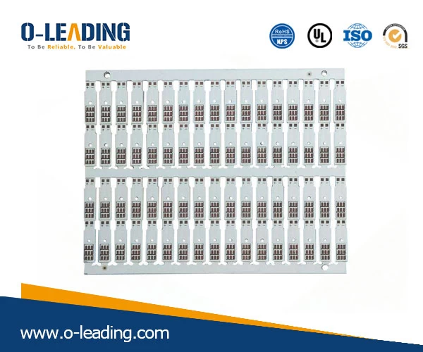
To reduce EMI, avoid forming traces, vias, and other components at a 90 ° angle, as right angles can radiate. Capacitance will increase at this corner, and the characteristic impedance will change, resulting in reflection and then EMI. To avoid 90 ° angles, traces should be routed at least two 45 ° angles to the corners.
Use caution with vias
In almost all PCB layouts, vias must be used to provide conductive connections between different layers. PCB layout engineers need to be careful because vias can create inductance and capacitance. In some cases, they also cause reflections because the characteristic impedance changes when a via is made in a trace.
Also keep in mind that vias increase trace length and require matching. For differential traces, avoid vias as much as possible. If this cannot be avoided, vias should be used in both traces to compensate for delays in the signal and return path.
Cable and physical shielding
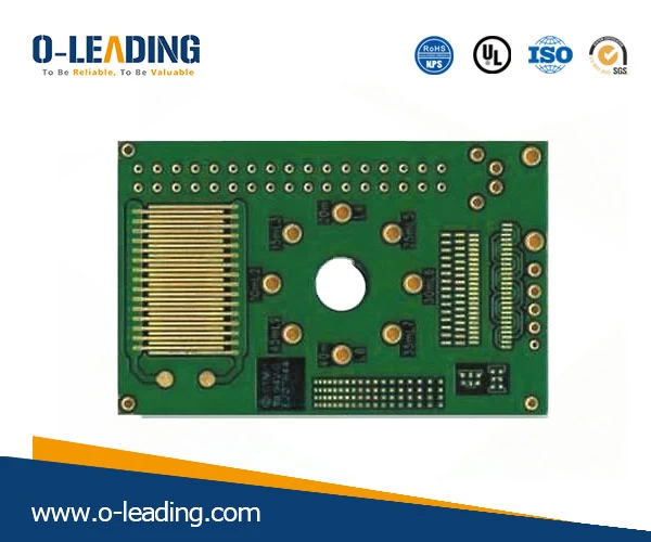
Cables carrying digital circuits and analog currents can generate parasitic capacitance and inductance, causing many EMC-related problems. If twisted-pair cables are used, the coupling level is kept low and the generated magnetic fields are eliminated. For high-frequency signals, shielded cables must be used, with the front and back sides grounded to eliminate EMI interference.
The physical shield is to cover the whole or part of the system with a metal package to prevent EMI from entering the PCB circuit. This shielding is like a closed, grounded conductive container that reduces antenna loop size and absorbs EMI.

