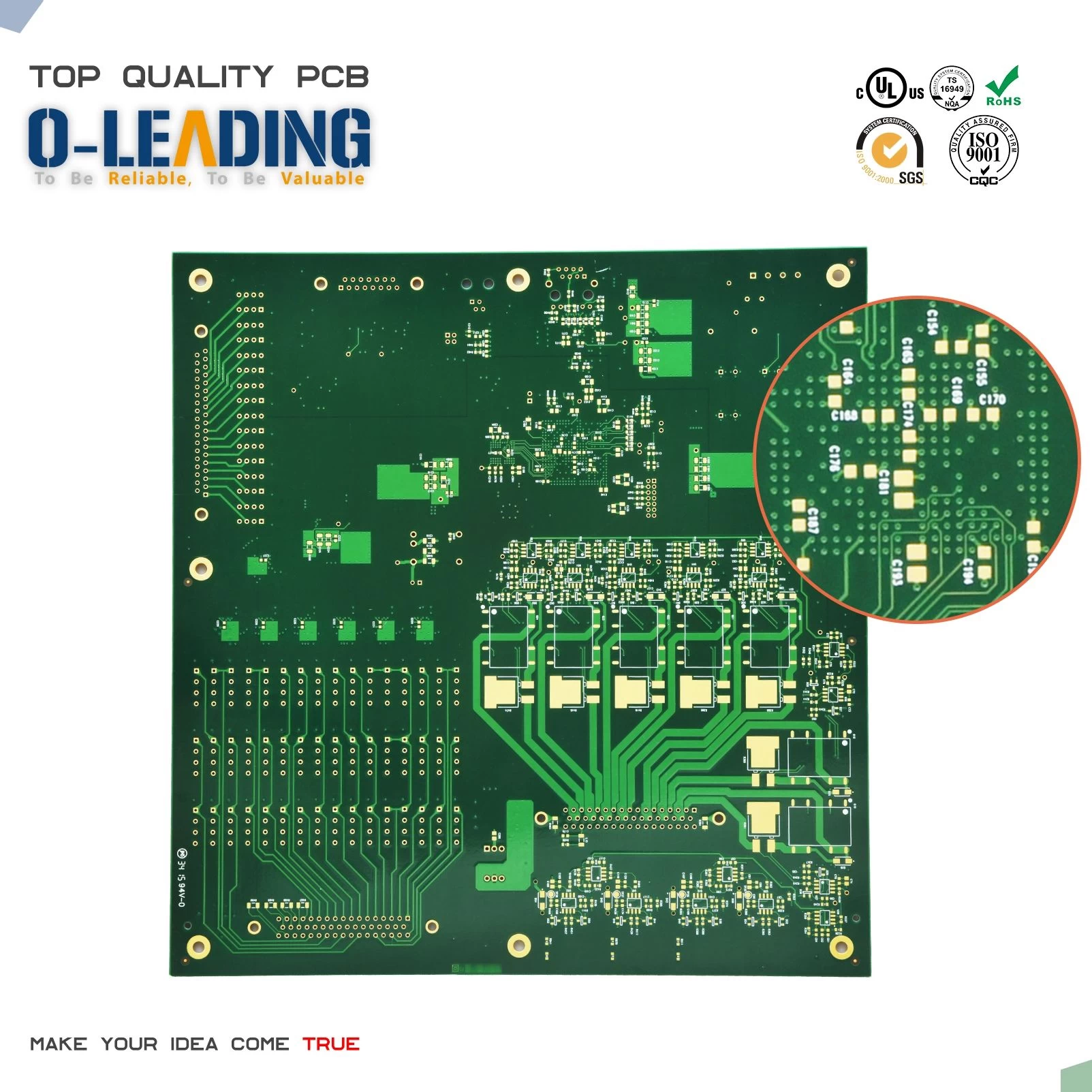
About PCB and assembly
o-leading.com
o-leading.com
2017-12-11 18:37:38
Technology about preventing the warping of PCB assembly Printed circuit board.
Why is the circuit board requirement very flat
In the automatic insertion line, if the printing circuit board is not flat, it will cause the location to be inaccurate, the components can’t be inserted into the hole and surface of the plate, and even the automatic plug loader.When the led pcb board Printed circuit board which assembled component is welded after soldering,and the foot of the element is difficult to be cut neatly.The PCB board also can’t be installed in the machine box or the socket in the machine, so, the pcb assembly factory meeting plate warped is also very troublesome.At present, the printing circuit board has entered the era of surface installation and chip installation, and the printed circuit board assembly plant must be more and more strict with the requirement of plate warped.
Standard and test methods for warp
According to the United States IPC-6012 (1996 edition) << rigid printed circuit board identification and performance specifications >>, the allowable maximum warping and distortion of the surface mounting plate is 0.75%, and all other pcb boards are allowed 1.5%.This has increased the requirements for the surface mounting plate board of the ipc-rb-276 (1992 version).At present, the warp degree of the license of each electronic pcb assembly plant, no matter double or multi-layer pcb, 1.6mm thickness, usually 0.70 ~ 0.75%, many SMT, BGA plate, the requirement is 0.5%.Some electronics factories are agitating for a 0.3 percent increase in warping standards, and the test warping measures follow gb4677.5-84 or ipc-tm-650.2.4.22b.Put PCB board on a verified platform, the test needle to warp degree of the largest local, to test the diameter of the needle, divided by the curve length of PCB board, warp degree of the printed circuit board can be calculated.
Standard and test methods for warp
Warping during manufacturing process
Engineering design: the design of the printing circuit board shall be noted:
A. The arrangement of the prepreg between the layers should be symmetrical, such as the six laminates PCB Board, the thickness of 1 ~ 2 and 5 ~ 6 layers should be consistent with the number of the semi-solidified pieces, otherwise the layer pressure will be easy to warp.
B. Multi-laminated core pcb and semi-cured tablets shall be used in the same supplier’s products.
C. The area of the outer A and B lines should be as close as possible.If A face is A large copper surface, and B is only A few lines, the plate is easy to warp after etching.If the two sides of the line area difference is too large, you can add some indifferent grid on the lean side, in order to balance.
If you want to learn more information about PCB, just click on pcb manufacturer in china.


