


- Contact Us
-
TEL: + 86-13428967267
FAX: + 86-4008892163-239121
+ 86-2028819702-239121
Email: sales@o-leading.com Contact Now
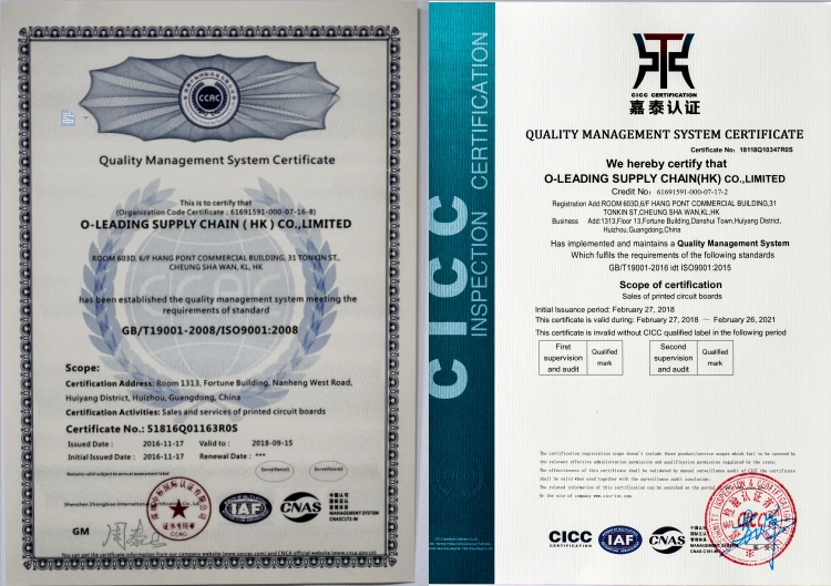
- Certifications
-


- Subscribe
-
Get email updates on new products
- New Products


- Electronic album


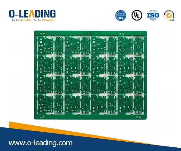

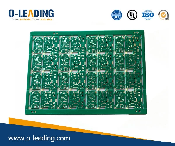
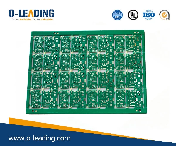
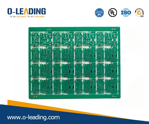
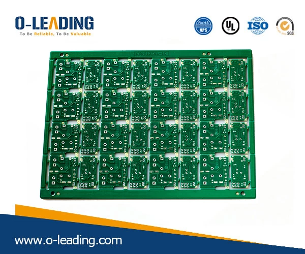
heavy copper pcb with 3oz
- PCB P/N: heavy copper pcb with 3/3oz
- Layer Count:2L
- Material:FR-4 TG130
- Board thk:1.00mm
- copper thk:3/3oz
- Smallest hole size:0.50mm
- No. of holes (pcs):106
- line w/s:10/10mil
| Welcome to O-leading |
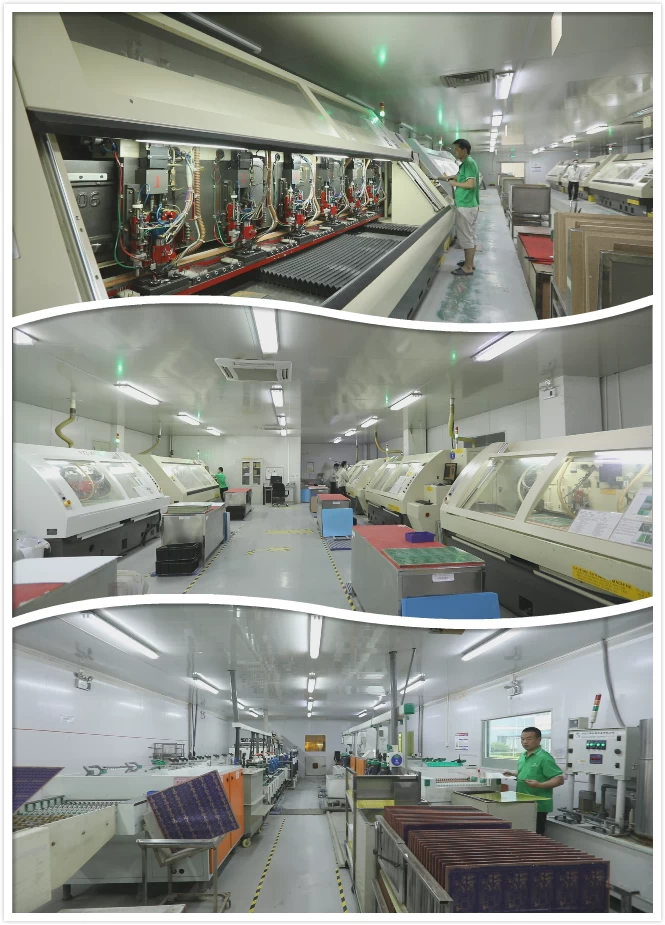
We are professional PCB manufacturer with more than ten years experiences . Products range-single, double side ,multi-layer PCB ,flexible PCB and MCPCB.We can provide fast prototype service – S/S in 24hrs , 4-8layers in 48-96 working hrs production time. (Thick copper pcb Manufacturer)
COPPER PLATE HOLES MINIMUM .025 AVG, .020 MIN.. HOLES MAY NOT BE PLUGGED
Pack with colorless transparent bubble film ,25 PCS/ bag, put desiccant in flank, put humidity indicator card on top side
PLEASE CLICK THESE FOR MORE INFORMATION: Thick copper pcb wholesales china
| Product Description |
| PCB P/N | heavy copper pcb with 3/3oz |
| Layer Count | 2L |
| Material | FR-4 TG130 |
| Board thk | 1.00mm |
| copper thk | 3/3oz |
| Smallest hole size | 0.50mm |
| No. of holes (pcs) | 106 |
| line w/s | 10/10mil |
| Impedance control. Y / N (Tol %) | N |
| Surface Finishing | LF-HASL |
| Solder Mask Silkscreen | Green/ N/A |
| Single board size | Dim X (mm): 44.5; Dim Y (mm): 34 |
| Panelisation | 198;Dim Y (mm):156;No Of UPS:16 |
| Special:peelable mask | N |
| Routing/Punching | CNC |

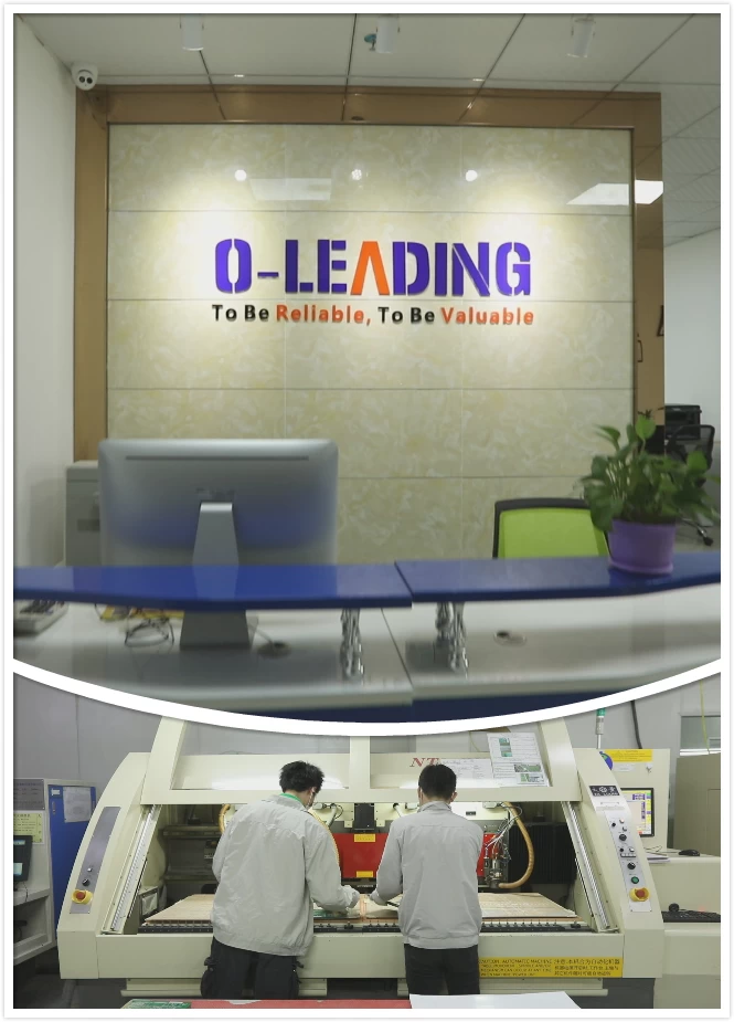
| Our Team |
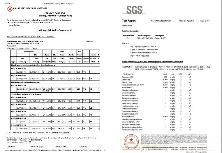
| Certifications |
| Packaging & Delivery |
| Packaging Details | 16 years professional OEM pcb board manufacturer |
| Delivery Detail | 7-12days |

| FAQ |
1. How do O-Leading ensure quality?
Our high quality standard is achieved with the following.
1.The process is strictly controlled under ISO 9001:2008 standards.
2.Extensive use of software in managing the production process
3.State-of-art testing equipments and tools. E.g. Flying Probe, X-ray Inspection, AOI (Automated Optical Inspector) and ICT (in-circuit testing).
4.Dedicated quality assurance team with failure case analysis process
5.Continuous staff training and education
2. How do O-Leading keep your price competitive?
Over the last decade, prices of many raw materials (e.g. copper, chemicals) had doubled, tripled or quadrupled; Chinese currency RMB had appreciated 31% over US dollar; And our labor cost also increased significantly. However, O-Leading have kept our pricing steady. This owns entirely to our innovations in reducing cost, avoiding wastes and improving efficiency. Our prices are very competitive in the industry at the same quality level.
We believe in a win-win partnership with our customers. Our partnership will be mutually beneficial if we can provide you an edge on cost and quality.
3. What kinds of boards can O-Leading process?
Common FR4, high-TG and halogen-free boards, Rogers, Arlon, Telfon, aluminum/copper-based boards, PI, etc.
4. What data are needed for PCB production?
It is best to provide data in Gerber 274-X format. In addition, Cam350, CAD, Protel 99se, PADS, DXP and Eagle can also be processed.
5. What’s the typical process flow for multi-layer PCB?
Material cutting → Inner dry film → inner etching → Inner AOI → Multi-bond → Layer stack up Pressing → Drilling → PTH → Panel Plating → Outer Dry Film → Pattern Plating → Outer etching → Outer AOI → Solder Mask → Component Mark → Surface finish → Routing → E/T → Visual Inspection.
- Other Products


