- Contact Us
-
TEL: + 86-13428967267
FAX: + 86-4008892163-239121
+ 86-2028819702-239121
Email: sales@o-leading.com Contact Now
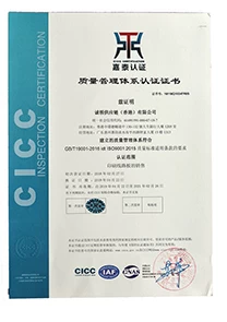
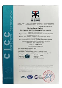
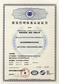
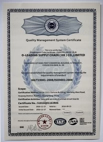
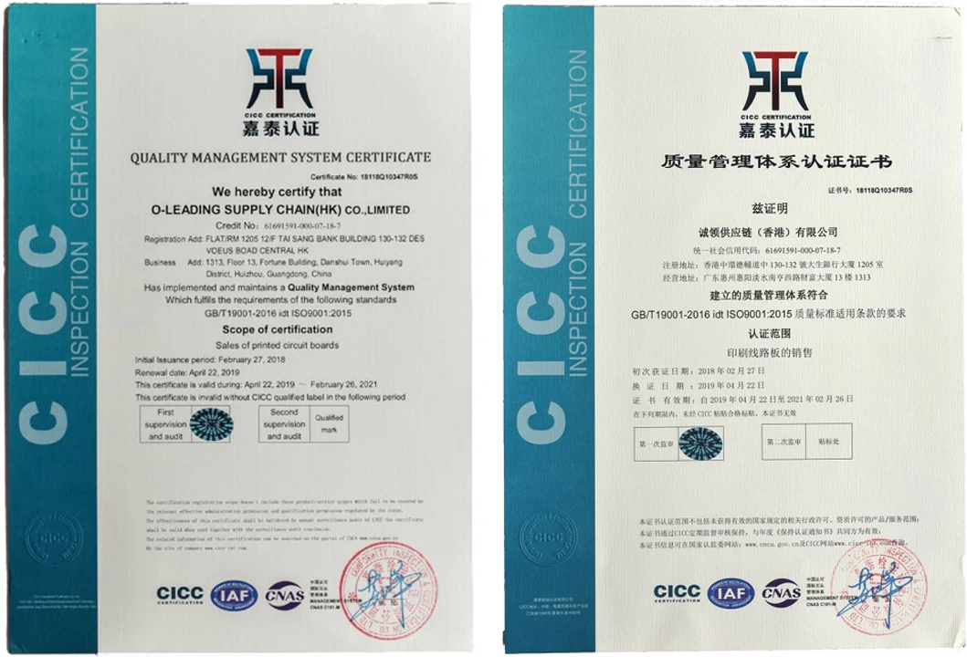
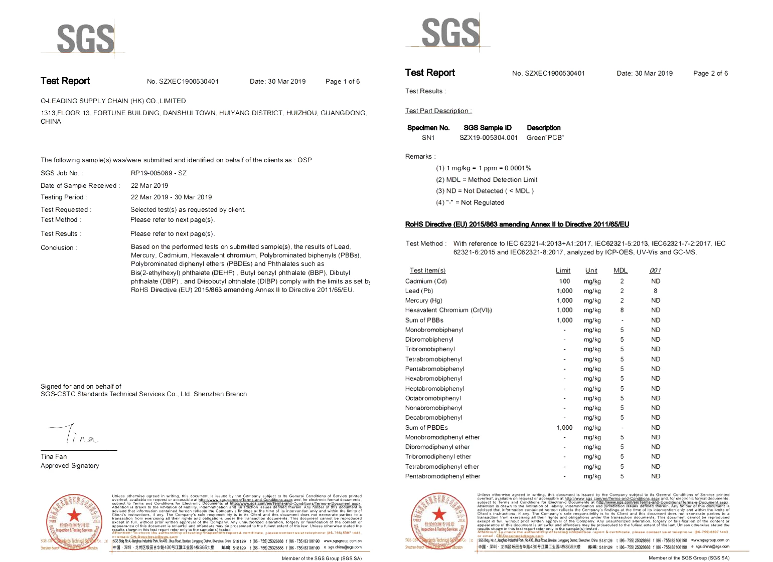
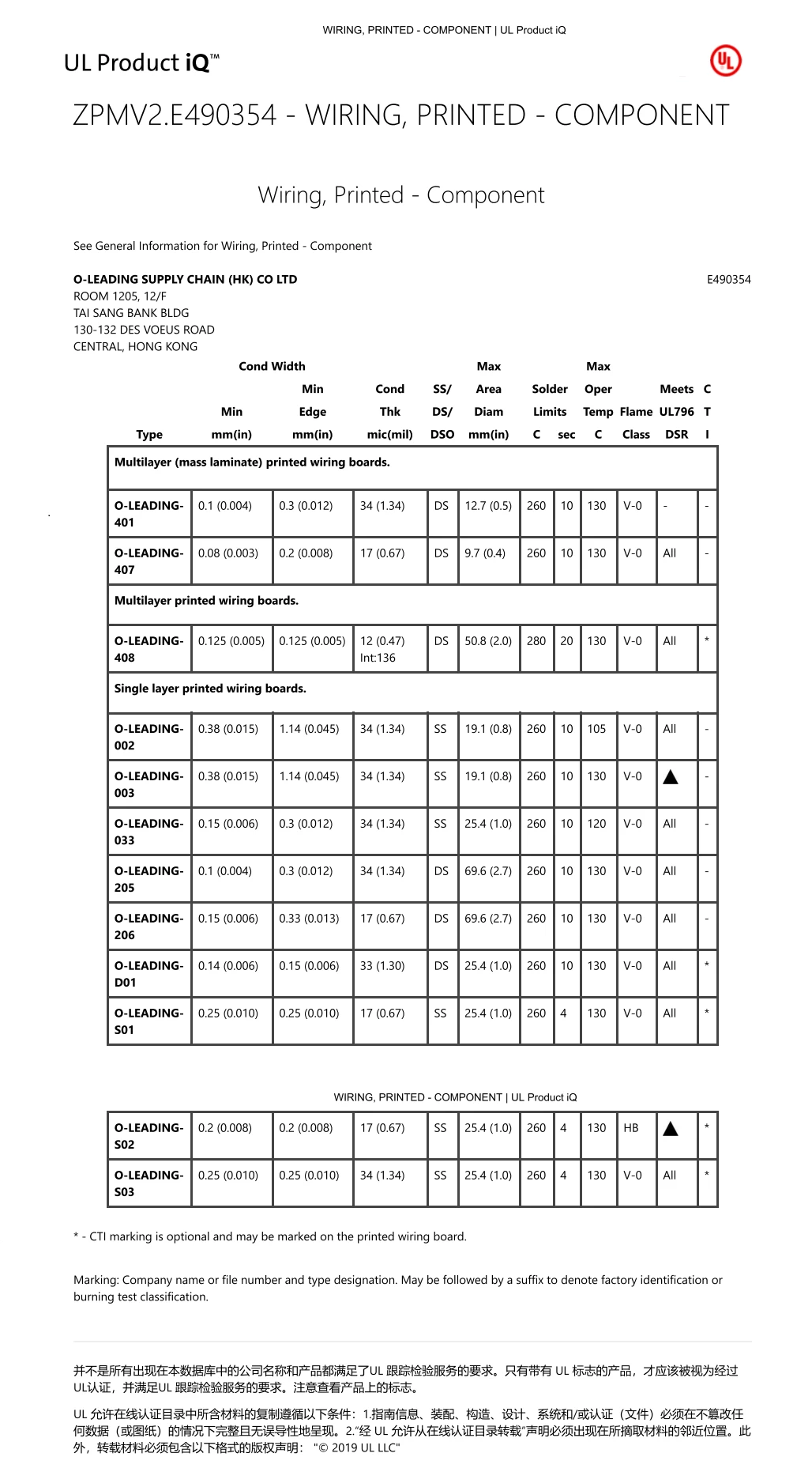
- Certifications
-
- Subscribe
-
Get email updates on new products
- New Products
-
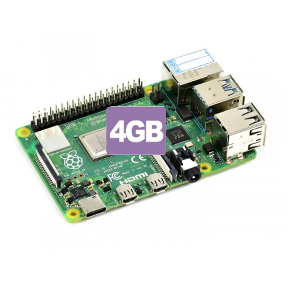
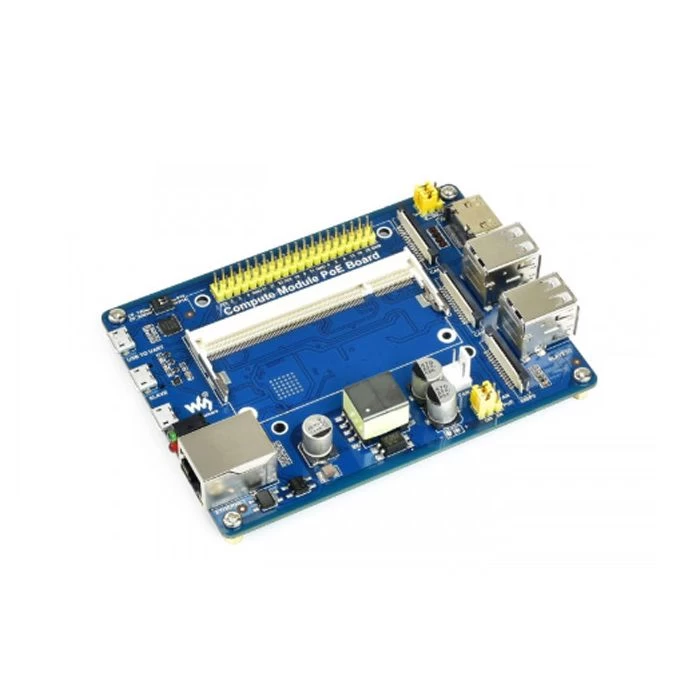
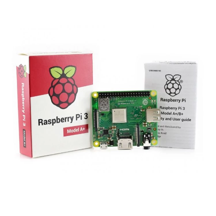
Faster Networking Multi-Media Capability Powerful Processor Completely Upgraded Raspberry Pi 4 Model B 4GB RAM
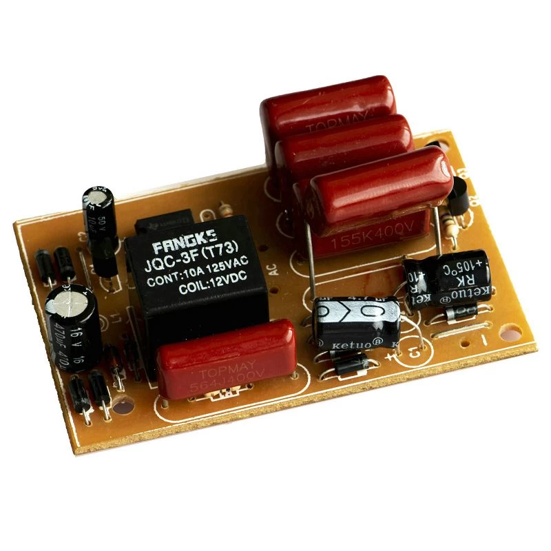
AC DC Power Supply 110V 220V to 5V 700mA 3.5W Switching Switch Buck Converter, Regulated Step Down Voltage Regulator Module
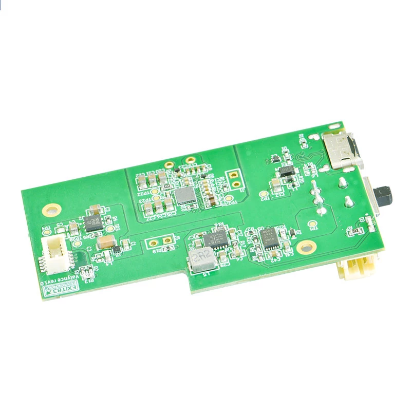
China Top 10 Electronic Power Pcba Suppliers, Printed Circuit Board Pcba Power Assembly Manufacturer, Service PCBA Power Factory
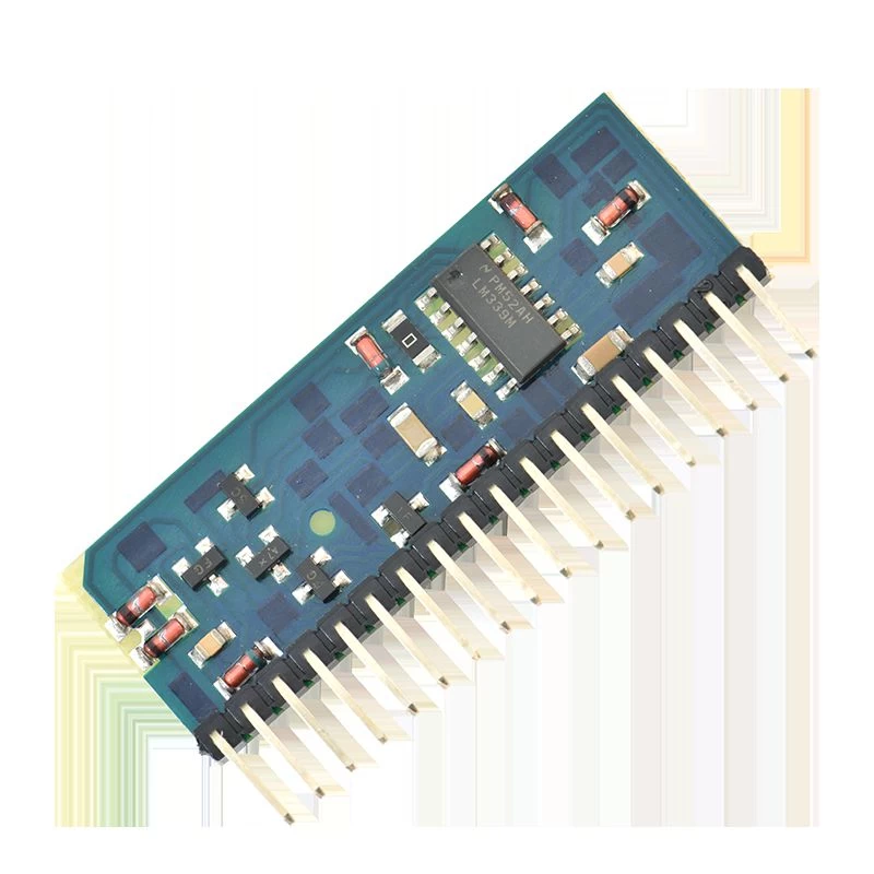
Fast delivery PCB One Stop Service Circuit Board Manufacture PCB Assembly PCBA PCB receiver control board
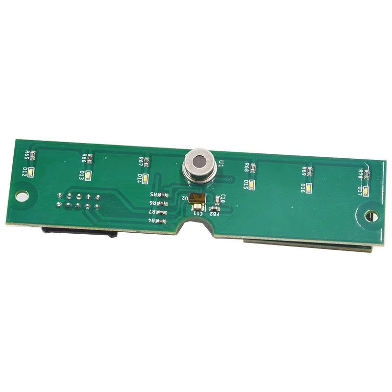
SMT OEM PCB Manufacturer PCBA Service PCB Assembly Electronics Printer Control Sanitise Dispense Sensor Board
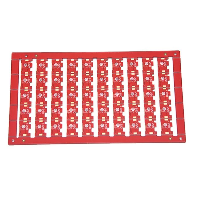
China Custom Multilayer PCB Board Service Half Plated Hold Wifi Module Small BGA Manufacturing Design
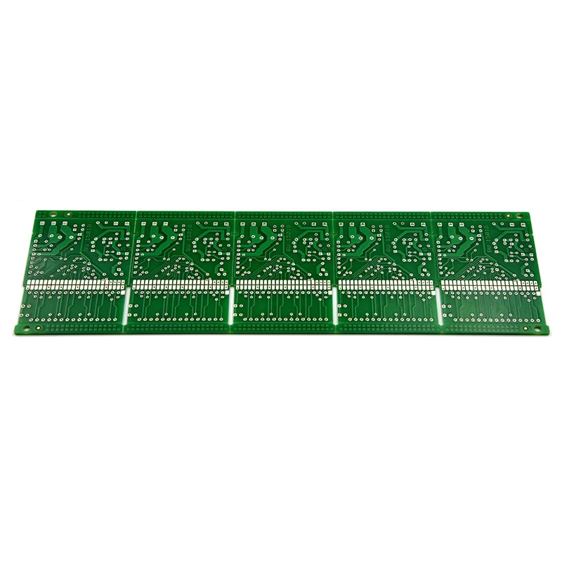
China Huizhou OEM Fast Lead Time Electronic PCB Board SMT Assembly PCBA Printed Circuit Board Manufacturer
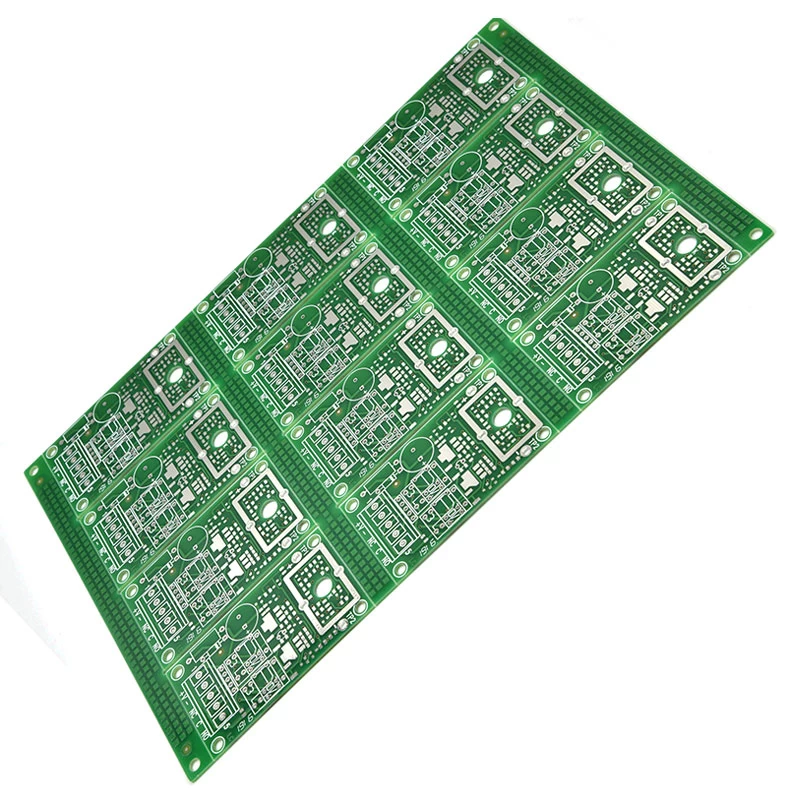
China Electronic Circuit Board PCB Assembly Board customized SMT PCBA fabricatio Printed Circuit Board
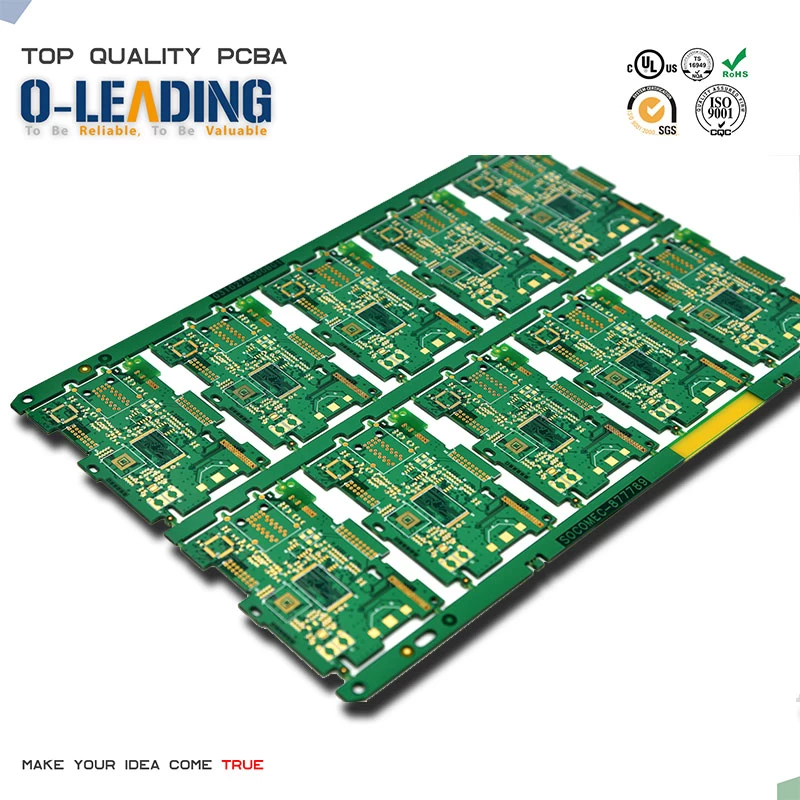
Factory Price 0.2 6mm Thickness Electronic Hardware Plating Circuit Board,Double Side Pcb Hard Gold Board Manufacturer
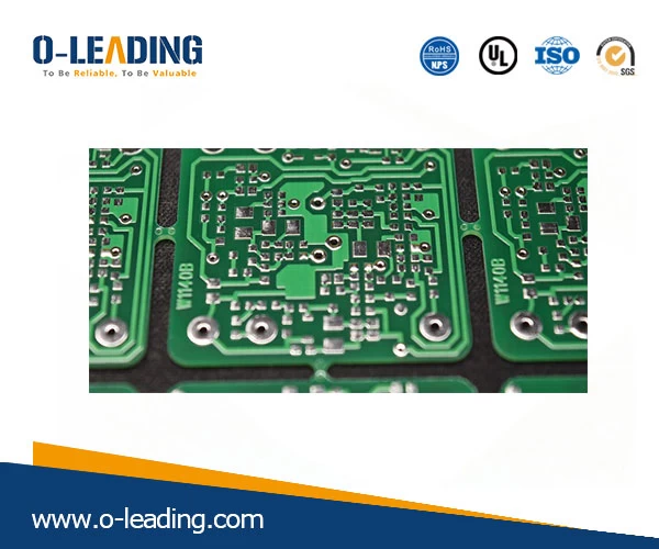
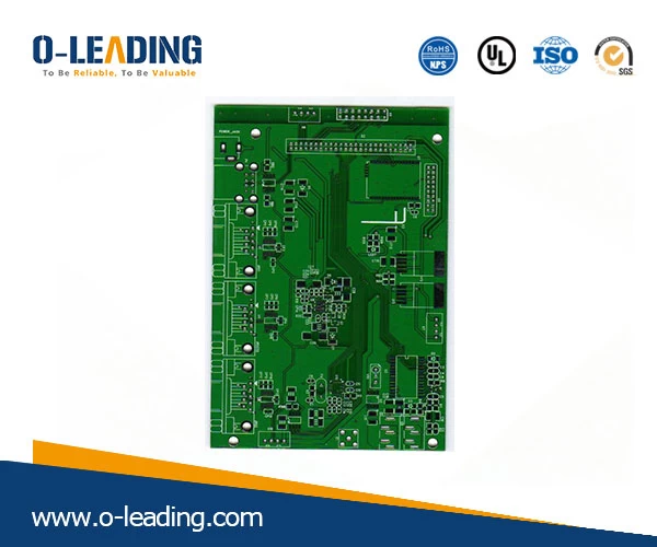
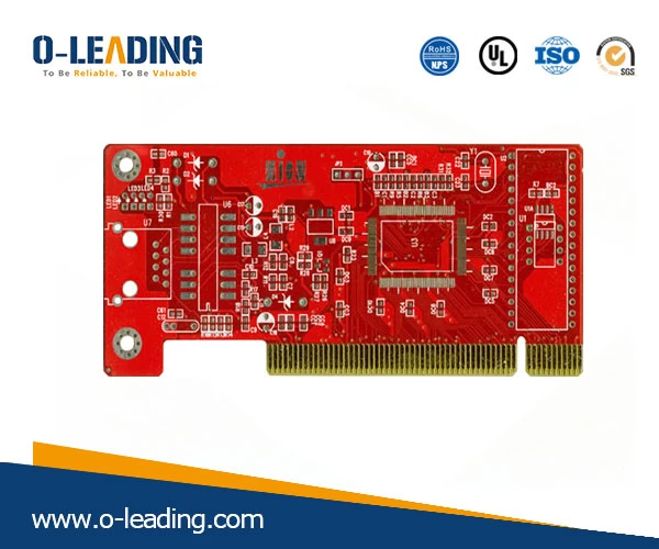
Production of printed circuit boards, manufacturer of Pcb China prototypes
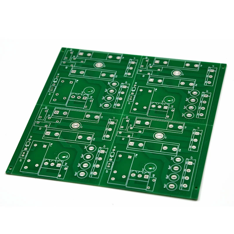
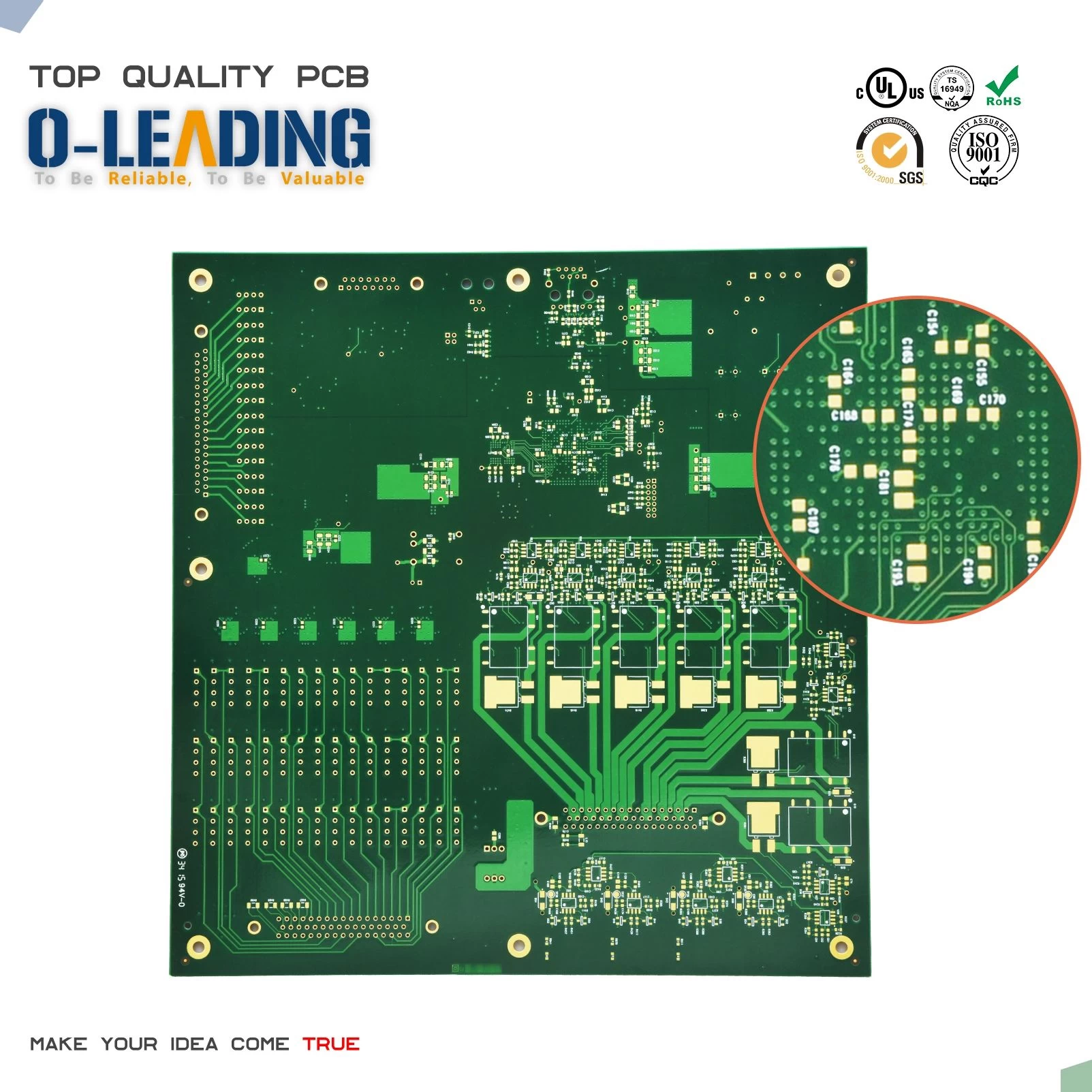
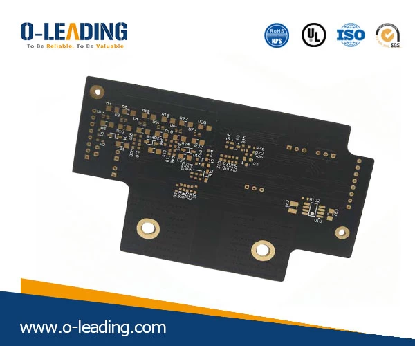
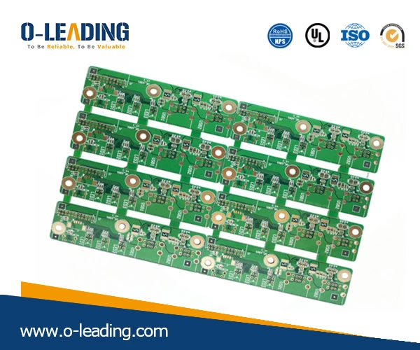
- P / N PCB: 104_DCP_R2
- Counting count: 4L
- Material: FR-4 TG130
- Board: 1.6 mm
- copper thk: 1/1/1 / 1oz
- Smallest hole size: 0.3 mm
- Number of holes (pcs): 295
- line without: 12 / 8mil
- Y / N impedance check (Tol%): N
- Surface finish: ENIG Au: 0.05-0.10UM
- Welding mask Serigraphy: green
- Single board size: Dim X (mm): 80; Dim Y (mm): 116
- Panelisation: Dim X (mm): 80; Dim Y (mm): 116; UPS No: 1
- Special: peelable mask: N
- Routing / punching: CNC
| Welcome to O-leading |
| Product Description |
|
Place of origin |
Guangdong, China (Mainland) |
Brand name |
O-leader |
|
Basic material |
FR-4, Aluminum |
Thickness of copper |
0.5 ounces - 5 ounces |
|
Min. Size of the hole |
0.2 mm |
Min. Width of the line |
0.2 mm |
|
Surface finish |
gold immersion, OSP, lead-free HASL |
Thickness of the table |
0.1-5mm |
|
Applicable to |
LED, cell phone, air conditioners, washing machines |
character |
Industrial control pcb |
|
certified |
ISO9001, UL, RoHS, SGS |
Q / CTN |
10PCS-100PCS |
|
weight |
0.01 kg -5 kg |
MOQ |
10 pieces |
| Model number | pcba manufacturer pcb assembly power bank | Min. Line spacing | 0.2 mm |
| color | blue, red, green, black, yellow | price | $ 0.1- $ 10 |
| type desigh | customer's requirement | cut it | 0.01m3-10m3 |
Product description
Professional manufacture of PCB boards for 16 years
|
article |
2014 |
2015 ~ 2016 |
2017 ~ 2018 |
|||
|
Volume |
Sample |
Volume |
Sample |
Volume |
Sample |
|
|
Counting of levels |
32 |
42 |
38 |
44 |
42 |
48 |
|
Line / space min (μm) |
50/50 |
40/45 |
40/45 |
40/40 |
35/40 |
35/35 |
|
Minimum hole |
00:15 |
00:10 |
00:15 |
00:10 |
00:15 |
00:10 |
|
Proportions |
14: 1 |
16: 1 |
16: 1 |
18: 1 |
18: 1 |
20: 1 |
|
N + C + N |
4 + C + 4 |
5 + C + 5 |
5 + C + 5 |
6 + C + 6 |
5 + C + 5 |
6 + C + 6 |
|
Any level interconnection |
5 + 2 + 5 |
6 + 2 + 6 |
5 + 2 + 5 |
6 + 2 + 6 |
5 + 2 + 5 |
6 + 2 + 6 |
|
Plate filling away |
YUP |
- |
YUP |
- |
YUP |
- |
|
Min. Core thickness (excluding copper) (μm) |
50 |
40 |
40 |
30 |
40 |
30 |
|
Min. Laser drill diameter (μm) |
75 |
65 |
65 |
50 |
50 |
40 |
|
Way up buried |
YUP |
- |
YUP |
- |
YUP |
- |
|
Material |
FR4, Megtron, Nelco, Rogers, heavy copper, etc. |
|||||
|
Built-in capacitor PCB |
YUP |
- |
YUP |
- |
YUP |
- |
|
Surface process |
Lead-free HASL, ENIG, OSP, silver by immersion, immersion pond, |
|||||
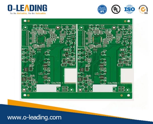

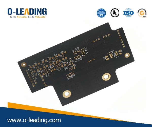
printed circuit board manufacturer
| Our Team |

| Certifications |
| Packaging & Delivery |

| Process Capability |
Layer Count: 1Layer-32Layer
Finished copper thickness: 1/3oz-12oz
Min Line width/spacing internal: 3.0mil/3.0mil
Min Line width/spacing external: 4.0mil/4.0mil
Max Aspect Ratio: 10:1
Board thickness: 0.2mm-5.0mm
Max Panel size(inches): 635*1500mm
Minimum Drilled Hole Size: 4mil
PIated Hole Tolerance: +/-3mil
BIind/Buried Vias (AII Types): YES
Via Fill(Conductive,Non-Conductive): YES
Base Material: FR-4,FR-4high Tg.Halogen free material,Rogers,Aluminium base,Polyimide,
PCB Material: FR-4,CEM-1,CEM-3,Aluminum-based board
Max PCB size: 510x460mm
Min PCB size:50x50mm
PCB Thickness:0.5mm-4.5mm
Board thickness:0.5-4mm
Min Components size: 0201
Standard chip size component: 0603 and larger
Component max height:15mm
Min lead pitch: 0.3mm
Min BGA ball pitch:0.4mm
Placement precision: +/-0.03mm

