


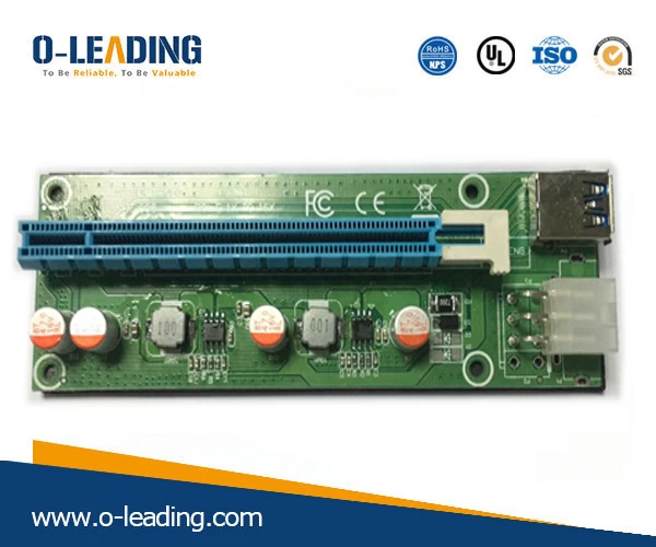
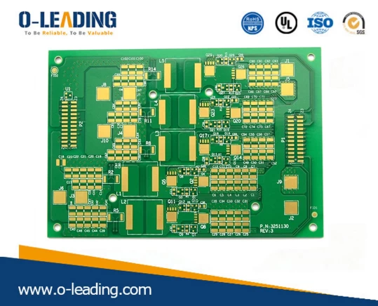
Interpretation of the meanings of each layer of the PCB board
o-leading.com
o-leading.com
2017-10-13 20:10:58
Topoverlay -- the top-level device name, also known as top silkscreen or top component legend, such as R1 C5.
IC10.bottomoverlay---- in multilayer----- if you design a 4 layer, you place a free pad or via, it is defined as multilay pad then it will automatically appear in the 4 layer, if you define it is top layer, then it will only appear in the top pad.
2G above high frequency PCB design, line, typesetting, should pay attention to what aspects?
High frequency 2G above PCB belongs to RF circuit design, not in the high-speed digital circuit design discussion range. The layout of radio frequency circuits (layout) and wiring (routing) should be considered together with schematic diagrams, because layout and routing can cause distributed effects. In addition, some passive components of RF circuits are designed by parameterization, and copper foil of special shape is realized. Therefore, EDA tools are required to provide parametric devices to edit copper foil of special shape. Mentor's boardstation has a dedicated RF design module that meets these requirements. Moreover, the general RF design requires a dedicated RF circuit analysis tools, the industry's most famous is the Agilent eesoft, and Mentor tools have a good interface.
2G high frequency PCB design, microstrip design should follow the rules?
The design of RF microstrip lines requires the use of 3D field analysis tools to extract transmission line parameters. All rules should be specified in this field extraction tool.