


PCB layout technology for optimizing power module performance
o-leading.com
o-leading.com
2017-07-09 12:10:17
The power to optimize the PCB ( power bank pcb board Printed ) capabilities of the power module and the lack of doubt about the dynamics of the global presence have led governments to vigorously promote the new energy conservation deal. The energy consumption standards of electronic products are becoming more and more severe, and the lack of doubt about the power of the whole world has made governments begin to popularize the new energy saving policies
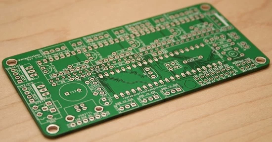
The energy consumption standards of electronic products are becoming more and more severe. As for power planning engineers, how to plan the power supply with higher power and higher functions is a permanent challenge. This article, starting with the power PCB ( china pcb manufacturer ) project, introduces the best PCB plan, examples, and skills for optimizing the SIMPLESWITCHER power module function.
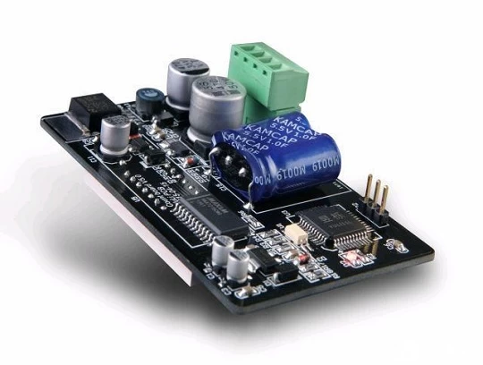
Minimizing inductance in the PCB ( HDI pcb Printed circuit board ) program has the following two advantages. First, by advancing the transmission of energy between the Cin1 and the CO1, component functionality is improved. This ensures that the module has outstanding high frequency bypass and minimizes the peak voltage of the inductance of the high di/dt current. Together with the equipment noise and voltage stress can be minimized to ensure its normal operation. Second, maximize the decline in EMI.
The energy consumption standards of electronic products are becoming more and more severe. As for power planning engineers, how to plan the power supply with higher power and higher functions is a permanent challenge. This article, starting with the power PCB ( china pcb manufacturer ) project, introduces the best PCB plan, examples, and skills for optimizing the SIMPLESWITCHER power module function.
Minimizing inductance in the PCB ( HDI pcb Printed circuit board ) program has the following two advantages. First, by advancing the transmission of energy between the Cin1 and the CO1, component functionality is improved. This ensures that the module has outstanding high frequency bypass and minimizes the peak voltage of the inductance of the high di/dt current. Together with the equipment noise and voltage stress can be minimized to ensure its normal operation. Second, maximize the decline in EMI.