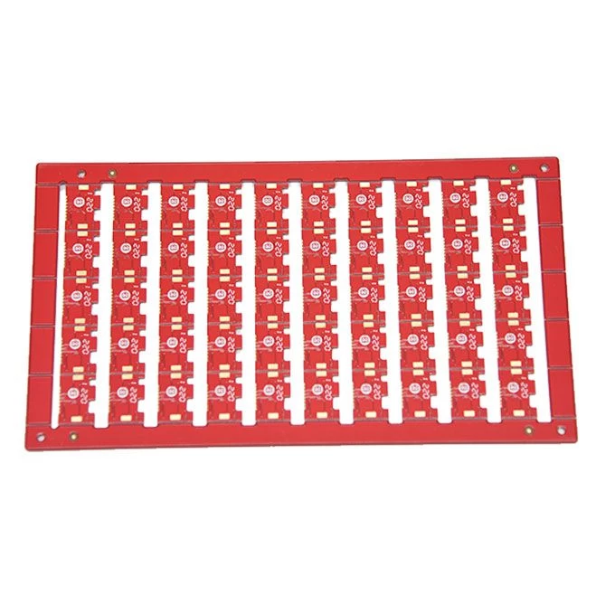
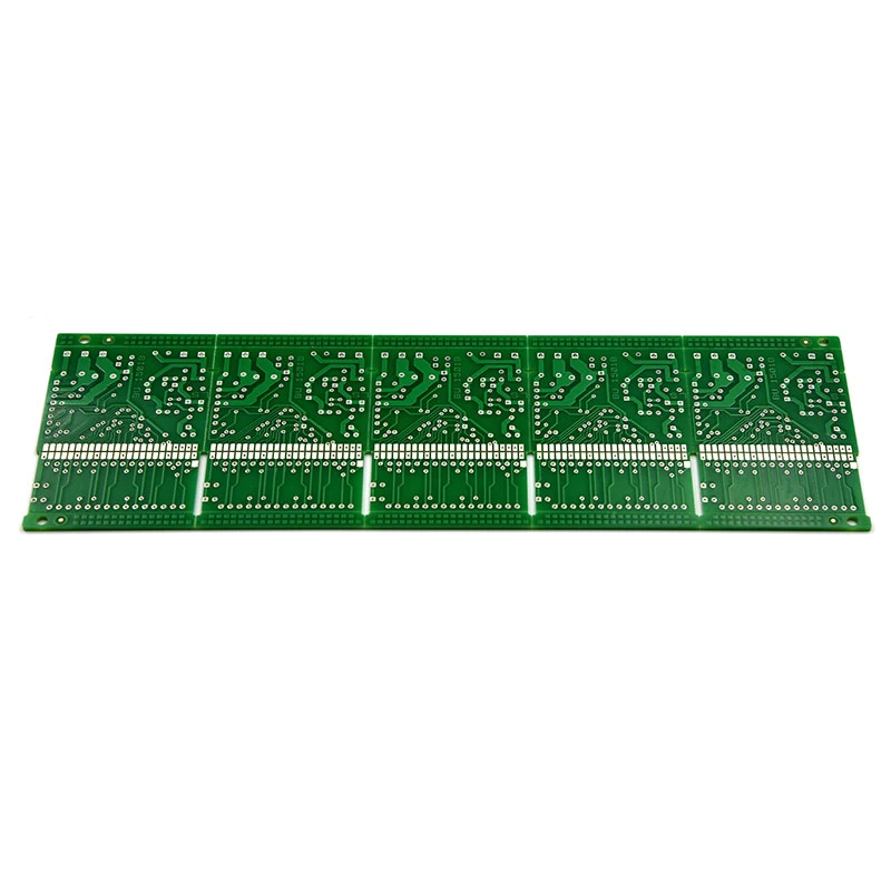
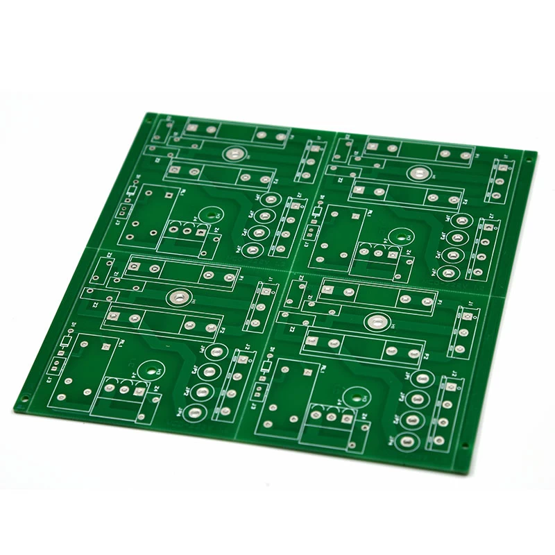
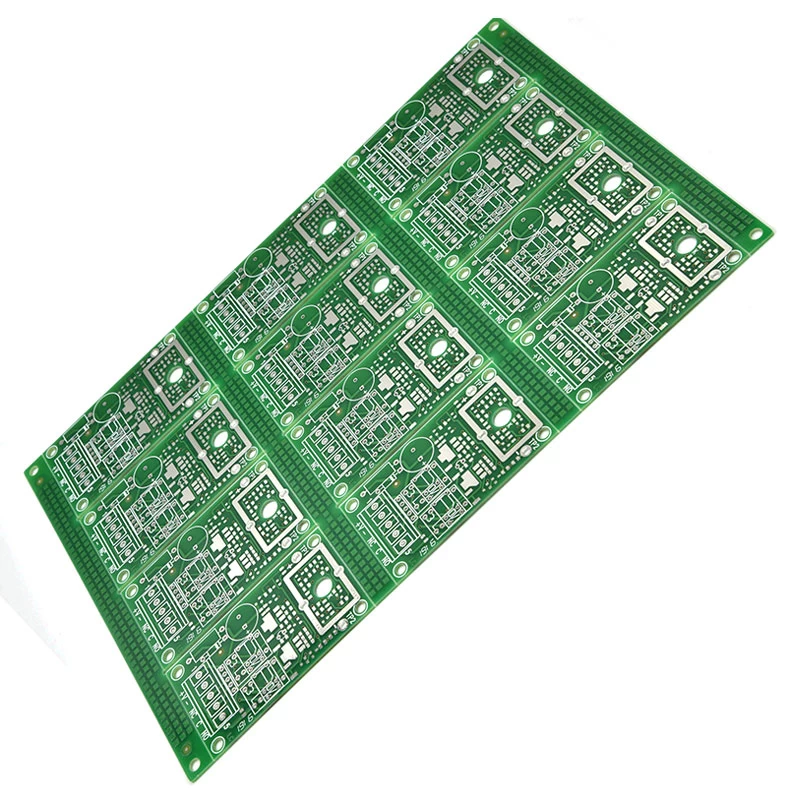
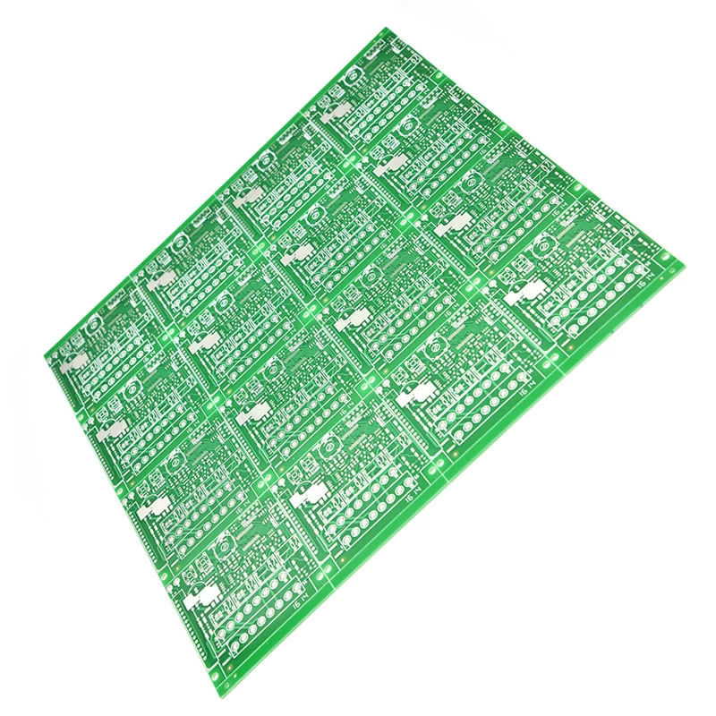
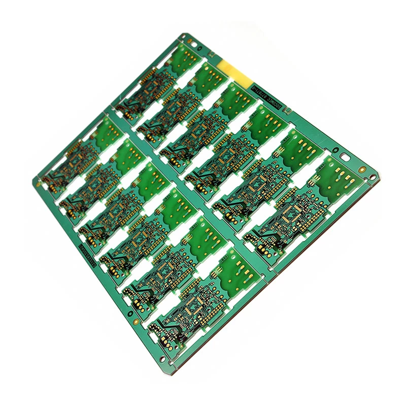
What is the PCBA processing flow?
2. Inspection of incoming materials of components, inspection of qualified warehouses, storage of warehouses;
3. According to product characteristics, customer requirements, select PCB board / BGA / IC baking, remove moisture;
4. Take out the solder paste and thaw it and stir it;
5.SMT patch;
6. Printing solder paste;
7. The PCB board after the completion of the patch needs to be reflowed;
8. AOI testing, first piece inspection;
9. DIP plugin, if the material needs to be shaped, it can be completed in this step;
10. Insert the PCBA board with wave soldering;
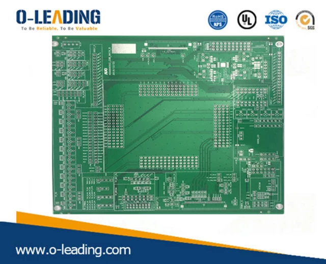
11. AOI inspection, post weld processing;
12. Clean the PCBA board;
13. Conduct tests, mainly ICT and FCT tests, ICT is line test, FCT is functional test, and functional test requires customer to provide test plan;
14. Apply three anti-paint according to customer requirements, the main purpose is to prevent moisture, moisture and shock;
15. Product assembly (depending on customer needs, this step is not required);
16. Choose the right packaging, package and ship.

