Printed circuit board layout
o-leading.com
o-leading.com
2017-12-21 10:53:43
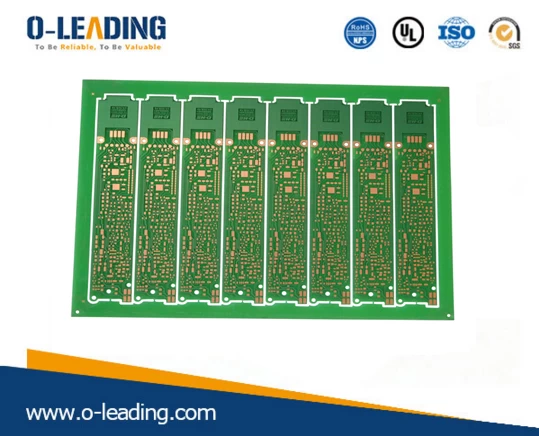
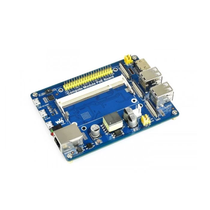
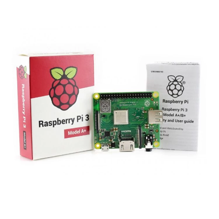
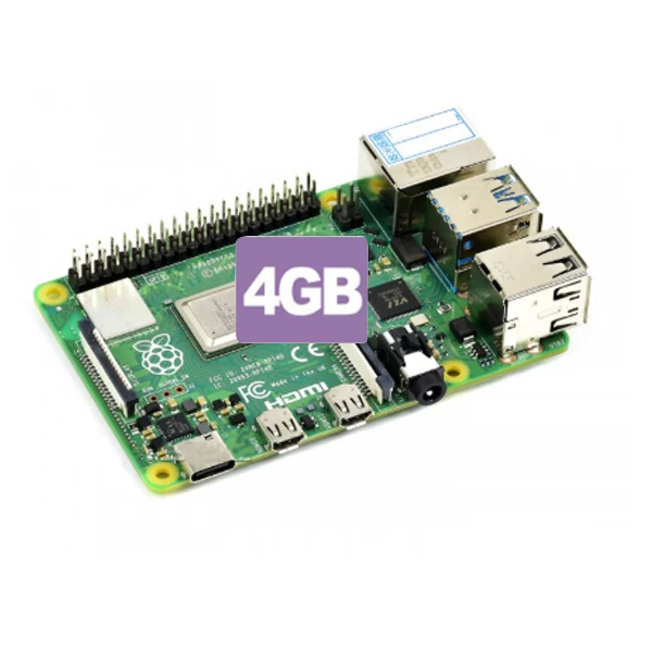
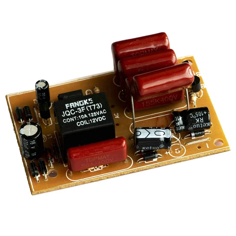
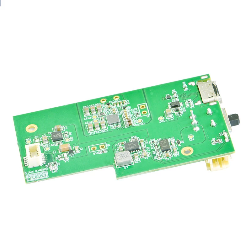
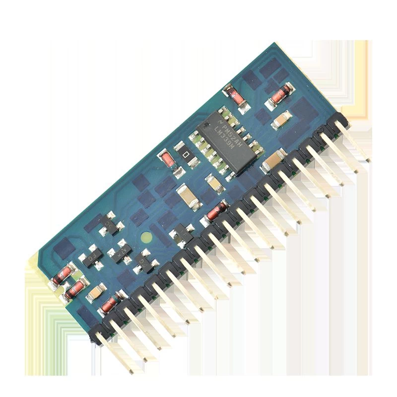
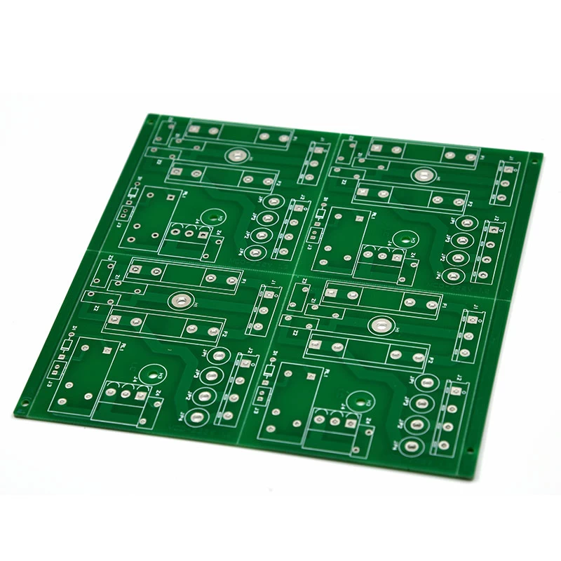
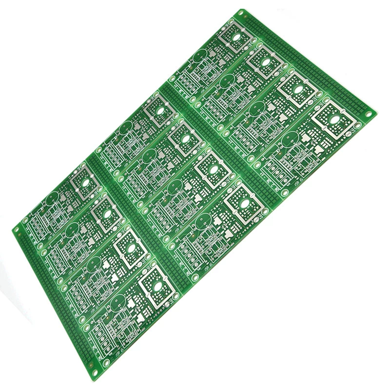
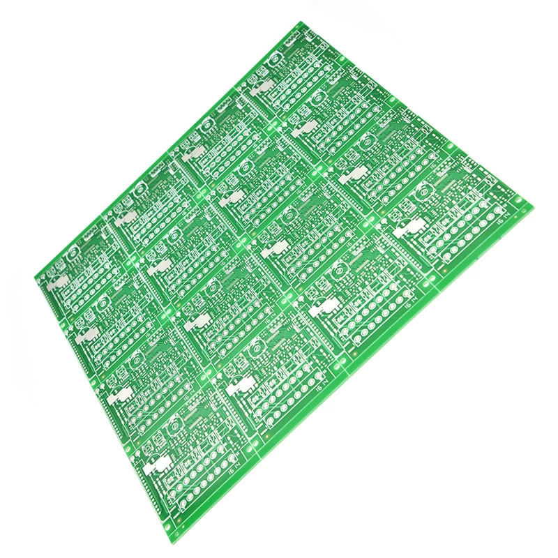
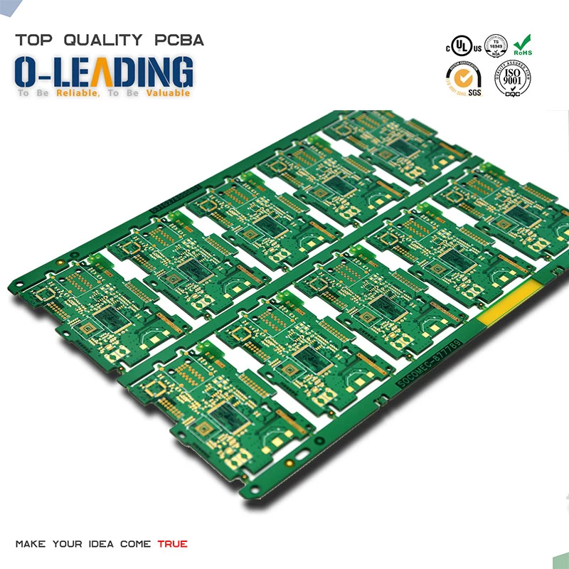
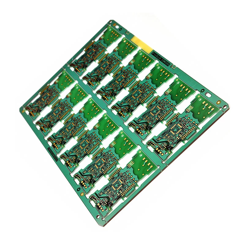
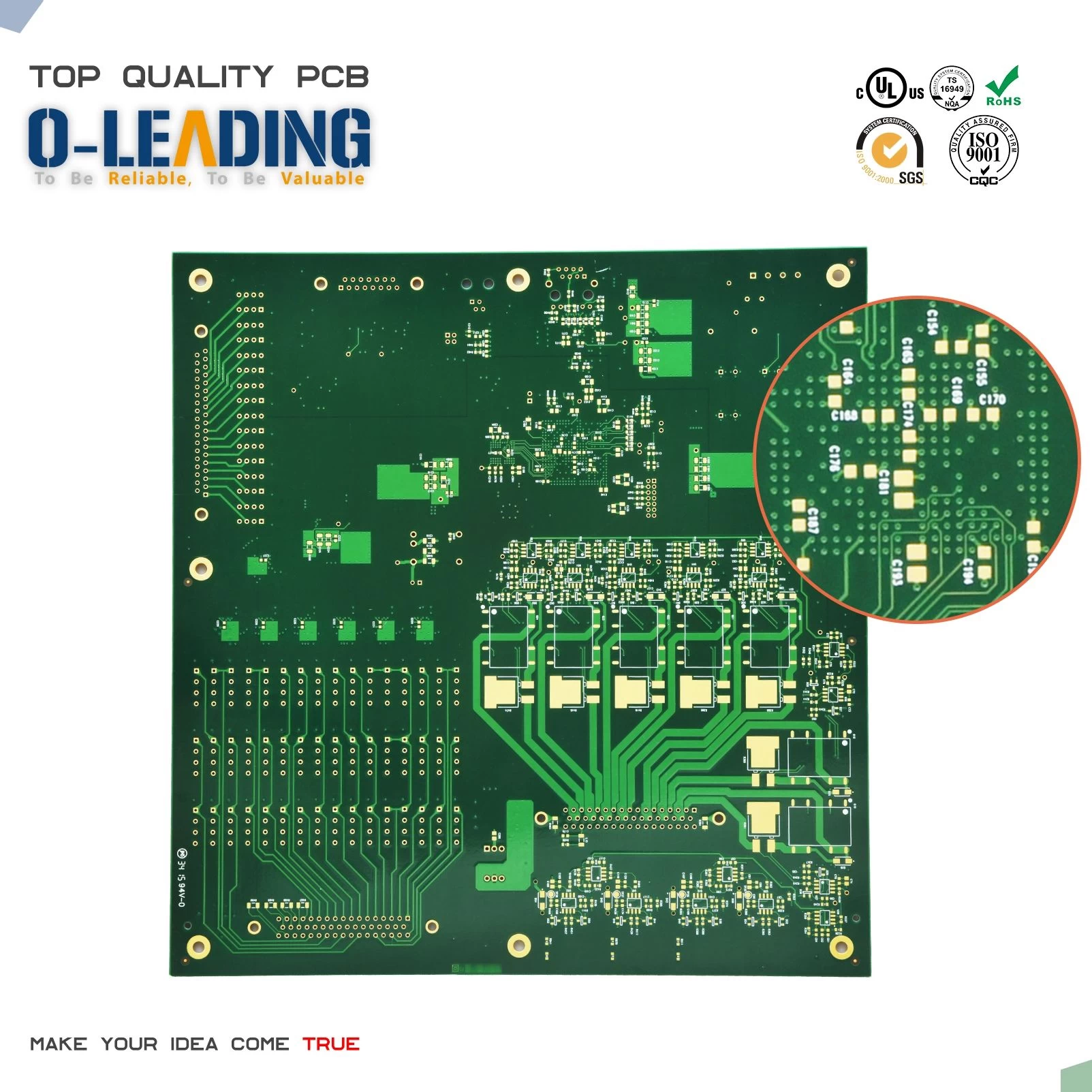
The printed circuit board is the laminate to which all the electronic components are soldered, with one or more layers of etched metal tracks making the connections. The components and connections in the printed circuit board layout are derived from the circuit design, and physically placed and routed by the designer using CAD software tools to get the best result. The connections on the printed circuit board should be identical to the circuit diagram, but while the circuit diagram is arranged to be readable, the printed circuit board layout is arranged to be functional, so there is rarely any visible correlation between the circuit diagram and the layout.
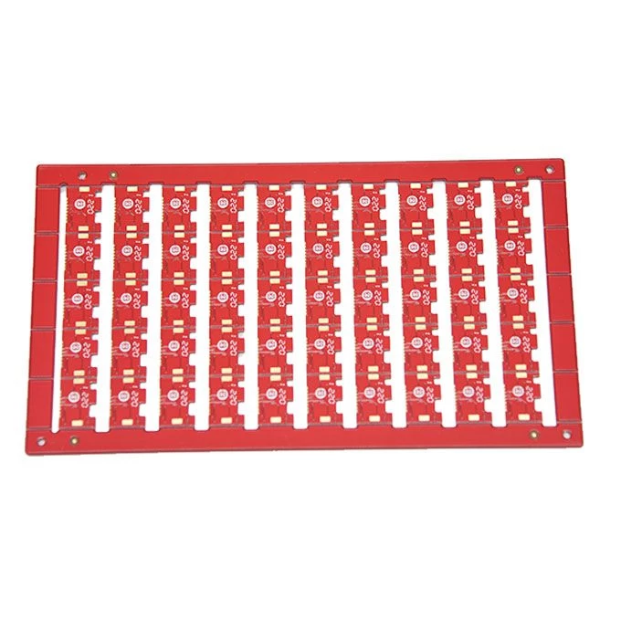
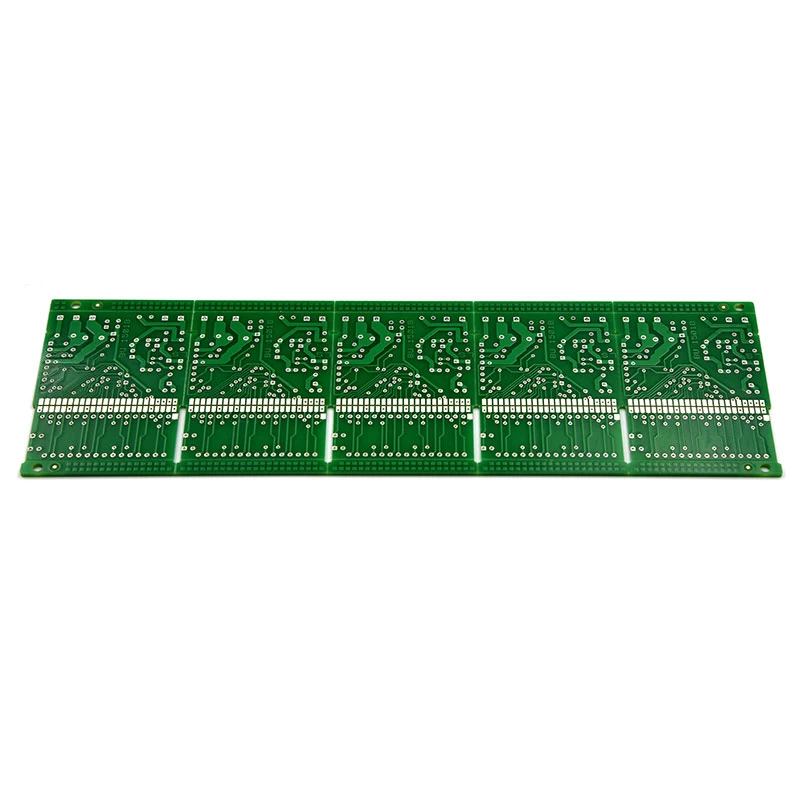
Printed circuit board layout can be performed manually using CAD or EDA tools or in combination with an auto-router. The best results are typically achieved using some combination of the two. The printed circuit board layout can consist of several layers and for illustration purposed the layers will be colored and compressed into a single overlay image. The width of the tracks is a trade-off based on current flow, space available, size of parts, and electromagnetic interference. The track layout is a similar trade-off that also picks when to dodge from one layer to another to avoid an obstacle, but generally aims to find the shortest path between the connected points. Given the impedance, susceptibility, and signal on tracks, the loop area is another trade-off that is considered as the design proceeds. And then, added to all that is design-for-manufacture or DFM. Please click china pcb manufacturer to get the information.
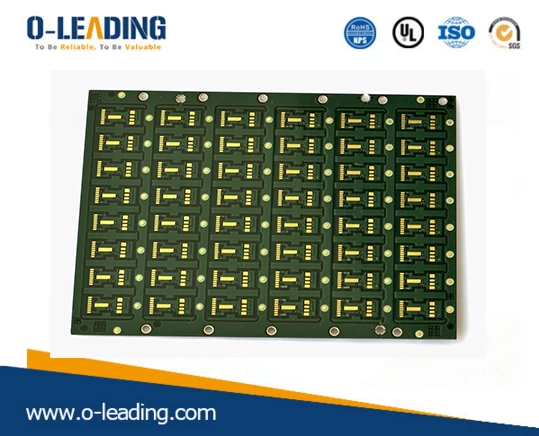
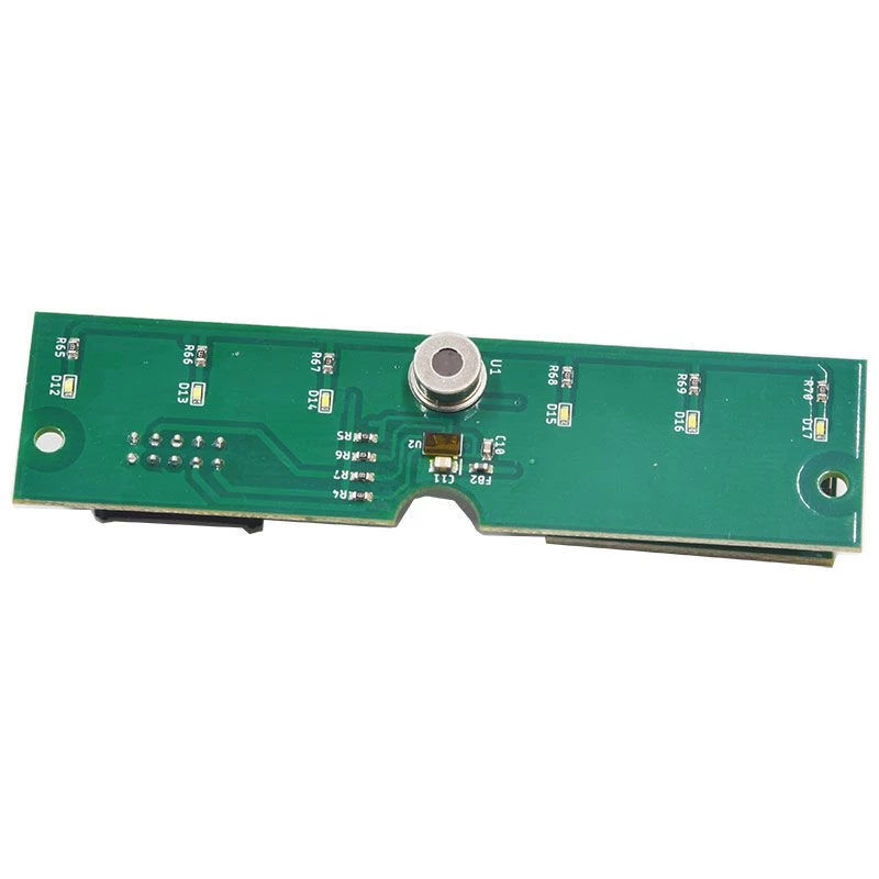
Printed circuit board manufacturer put a complete silkscreen identification overlay on most of our boards. The silkscreen contains important information that assists people to correctly assemble and use the device. When the printed circuit board layout is complete, the final CAD or Gerber file is sent for manufacturing. The etched printed circuit board is typically ready a few days later, ready for assembly into prototypes.

O-leading.com has worked with several companies and helped them bring their products to the market. Our highly skilled engineers have several years of experience in printed circuit board layout, which makes us an ideal choice for all types of design projects. Our clients range from start-ups who need a few printed circuit board prototypes, to large established corporations who need several thousand multi-layered circuit boards, and everything in between. So whatever your requirements may be, we are just a phone call away.
Printed circuit board layout can be performed manually using CAD or EDA tools or in combination with an auto-router. The best results are typically achieved using some combination of the two. The printed circuit board layout can consist of several layers and for illustration purposed the layers will be colored and compressed into a single overlay image. The width of the tracks is a trade-off based on current flow, space available, size of parts, and electromagnetic interference. The track layout is a similar trade-off that also picks when to dodge from one layer to another to avoid an obstacle, but generally aims to find the shortest path between the connected points. Given the impedance, susceptibility, and signal on tracks, the loop area is another trade-off that is considered as the design proceeds. And then, added to all that is design-for-manufacture or DFM. Please click china pcb manufacturer to get the information.

Printed circuit board manufacturer put a complete silkscreen identification overlay on most of our boards. The silkscreen contains important information that assists people to correctly assemble and use the device. When the printed circuit board layout is complete, the final CAD or Gerber file is sent for manufacturing. The etched printed circuit board is typically ready a few days later, ready for assembly into prototypes.
