


Cause analysis of PCB deformation
o-leading.com
o-leading.com
2017-09-12 20:12:30
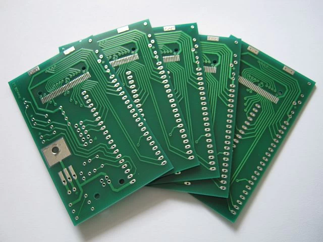
PCB (Printed circuit board in china) board consists of copper foil, resin, glass cloth and other materials, and the physical and chemical properties of each material are different. After pressing together, the residual stress will be generated, resulting in deformation. At the same time during the processing of PCB, after high temperature, mechanical cutting, wet processing and other processes, will also have an important impact on plate deformation, the cause of PCB (Printed circuit board manufacturer) plate deformation is complicated, how to reduce or eliminate the deformation caused by different material properties or processing, has become one of the PCB manufacturers face the most complex the problem.
Cause analysis of deformation
The uneven surface of the copper plate on the circuit board will worsen the bending and bending of the board.
The connecting point of each layer of the circuit board (vias, vias) will limit the board.
The weight of the board itself will cause the board to sag
The depth of the V-Cut and the connecting bars will affect the amount of deformed panels