


Do you know PCB surface treatment?
o-leading.com
o-leading.com
2017-06-19 10:42:25
Custom Circuit Boards china in the electronics industry has occupied an absolute dominance. Do you know what the purpose of PCB surface treatment is, what is the current situation? Here I will briefly introduce its purpose and status quo.
PCB surface treatment is the most basic purpose is to ensure good solderability or electrical properties. As the natural copper in the air tend to exist in the form of oxides, is unlikely to remain long-term for the original copper, so the need for other treatment of copper.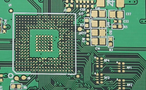
pcb board manufacture china PCB surface treatment process there are many, but with the human living environment requirements continue to improve, PCB performance process involved in the environmental problems is particularly prominent. The current topic of lead and bromine is the hottest, lead-free and halogen-free will affect PCB development in many ways. In the case of increasingly high environmental protection, PCB surface treatment process will certainly change the future.
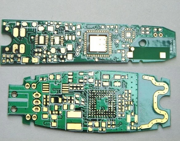
The inventor of the single-sided PCB circuit board was Austrian Paul Eisler, who used a printed circuit board in a radio device in 1936. Since the mid-1950s, single-sided PCB circuit board technology has been widely used. In general, single-sided PCB circuit board is copper-plated through the etching process. Copper plate by the board and copper foil composition, the board is usually made of glass fiber and other insulating materials, covered with a layer of copper foil (usually using oxygen-free copper). Copper foil after etching left a section of twists and turns of the copper foil, these copper foil called the alignment. The functions of these traces are equivalent to those in the circuit schematic, which are responsible for connecting the components of the components together. There are holes in the copper foil, used to install electronic components, known as drilling. While the copper foil used for soldering with the component pins is called a pad.
 Obviously, single-sided PCB circuit board for electronic components to provide fixed, assembled mechanical support, electronic components can be achieved between the electrical connection or insulation. In addition, we can see many single-sided PCB circuit board are printed on the component number and some graphics, which for the components of the plug, inspection, maintenance provides a convenient.
PCB surface treatment is the most basic purpose is to ensure good solderability or electrical properties. As the natural copper in the air tend to exist in the form of oxides, is unlikely to remain long-term for the original copper, so the need for other treatment of copper.
The inventor of the single-sided PCB circuit board was Austrian Paul Eisler, who used a printed circuit board in a radio device in 1936. Since the mid-1950s, single-sided PCB circuit board technology has been widely used. In general, single-sided PCB circuit board is copper-plated through the etching process. Copper plate by the board and copper foil composition, the board is usually made of glass fiber and other insulating materials, covered with a layer of copper foil (usually using oxygen-free copper). Copper foil after etching left a section of twists and turns of the copper foil, these copper foil called the alignment. The functions of these traces are equivalent to those in the circuit schematic, which are responsible for connecting the components of the components together. There are holes in the copper foil, used to install electronic components, known as drilling. While the copper foil used for soldering with the component pins is called a pad.