


Past and future trends in PCB design
o-leading.com
o-leading.com
2017-06-27 15:10:28
Over the years, PCBs have undergone significant changes in assembly, design, manufacturing and prototyping. Pcb design in china is critical to its performance, especially in complex devices. Hence we decided to share with you some of the changes that have taken place in the PCB industry especially for the design section over the years and the anticipated future changes and improvements in PCB design.
PCB design can be traced back to the era where only single-sided boards with no surface mount components were used. In the late ‘70s, most boards were designed using tapes to represent pads and traces. The Mylar sheet was used as the Printed Circuit Board. In the ‘80s, the double-sided boards which lacked the SMT and whose second sides were made of copper not components were introduced in the market.
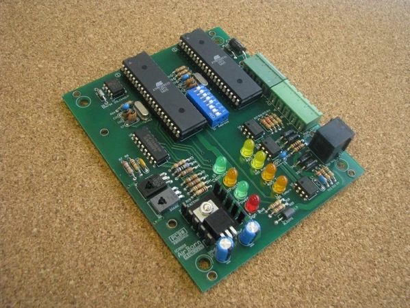
A different PCB design method also existed during the same age in different Printed circuit board company. This method used a material known as Rubylith which was polyester covered with a red plastic laminate. Design of such boards involved the use of an X-Acto knife for removing the red where pads and traces would be. The negatives were then used to produce a board on the photoresisor-coated blanks. The using of the SMTs made PCB design much simpler. Therefore, an explosion of different types of packages began to appear in the market. One such package is the BGA package which led to a massive increase in multilayer boards meaning that boards could now be packed with components thus they became more functional and smaller.
It is clear that PCB design has improved over the years especially from 1994. This is due to the introduction of more efficient PCB design software and the TLA program.
PCB miniaturization and increase in PCB density implies that components benefit from large scale integration hence the component count on the boards reduces significantly. Moreover, the size of components is reducing each day thus the clock speeds increase leading to generation of more heat thus special mounting requirements for chips will be one of the major strides expected to be introduced in the market soon with both electrical and mechanical engineering designers working together. This is because thermal issues are both electrical in terms of power losses and consumption and a mechanical problem in terms of the means of channeling the heat away from the components.
PCB miniaturization and increase in PCB density implies that components benefit from large scale integration hence the component count on the boards reduces significantly. Moreover, the size of components is reducing each day thus the clock speeds increase leading to generation of more heat thus special mounting requirements for chips will be one of the major strides expected to be introduced in the market soon with both electrical and mechanical engineering designers working together. This is because thermal issues are both electrical in terms of power losses and consumption and a mechanical problem in terms of the means of channeling the heat away from the components.
Designers are currently designing circuit components like touch sensors on the PCBs to reduce their net cost. However, this design technique has the challenge when it comes to the creation and scaling of the complex shapes required for the implementation of components. A convergence of PCB functionality into FPGA (Field-Programmable Gate Arrays) which leads to lesser costs of PCBs and higher functionality is expected to dominate the market soon although this method has traditionally been used as the realm of specialist designers. Introducing it in the general markets helps in shifting economics in favor of programmable devices since it will replace the discrete 32-bit microcontroller and its associated peripheral chips. PCB design has a brighter future can be predicted.