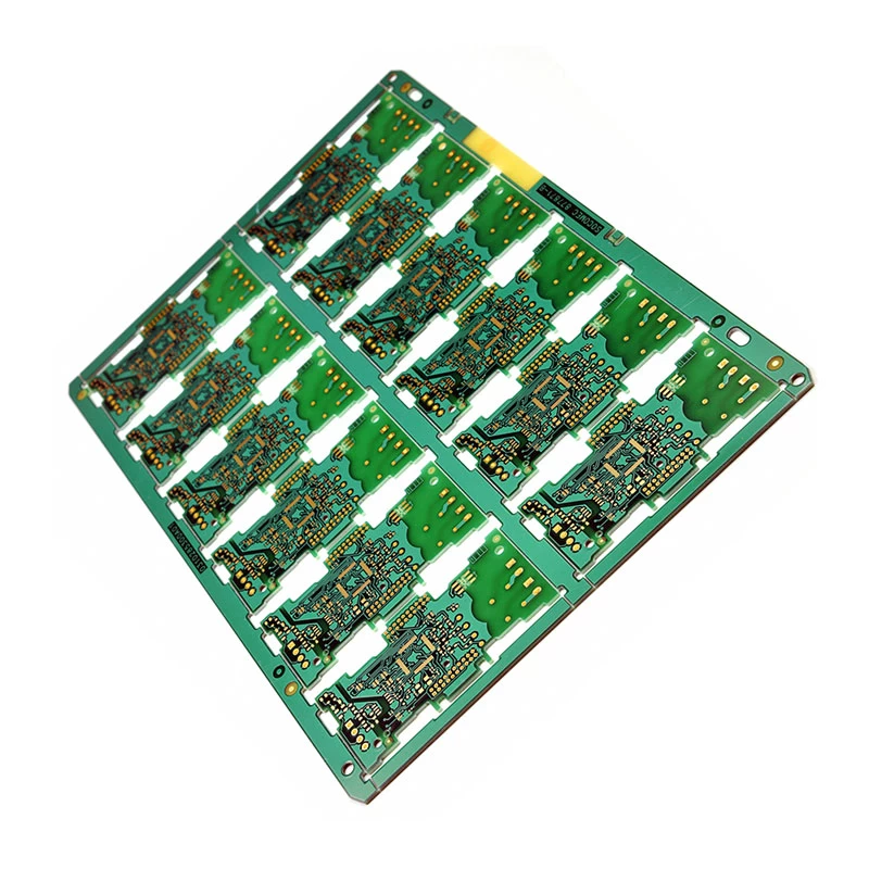
PCB layered design
1. The reference surface should preferably be planar. Both the power supply and the ground plane can be used as reference planes, and both have a certain shielding effect. However, the power plane has a relatively high characteristic impedance and a large potential difference from the reference ground level, and the shielding effect is much lower than the ground plane.
2. Layered circuits and analog circuits. Where design costs permit, it is best to arrange the digital and analog circuits on different layers. If it must be arranged on the same wiring layer, it can be remedied by ditching, adding grounding lines, dividing lines, etc. The analog and digital power and ground must be separated and must not be mixed.
3. The key signal traces of adjacent layers do not cross the partition. The signal span will form a large signal loop that produces very strong radiation. If the signal line has to be spanned in the case of grounding, a single point connection between the divided grounds may be first formed to form a bridge between the two grounds, and then routed through the bridge.
4. There must be a relatively complete ground plane below the component surface. The integrity of the ground plane must be maintained as much as possible for the multilayer board, and signal lines are generally not allowed to be routed in the ground plane.

5.High-frequency, high-speed, clock and other key signal lines should have adjacent ground planes. The distance between the signal line and the ground line thus designed is only the distance between the PCB layers, so the actual current always flows on the ground line directly below the signal line, forming a minimum signal loop area and reducing the radiation.


