


PCB design pad types and design standards
In PCB design, the pad is a very important concept, PCB engineers must be familiar with it. However, despite their familiarity, many engineers have little knowledge of pads.
One: pad type
In general, the pads can be divided into 7 categories, according to the shape as follows:
Square pads-printed board with large and few components, and printed wires are often used, when using PCBs by hand, this pad is easy to implement.
Round pads-widely used in single and double-sided printed boards with regularly arranged components. If the density of the board allows, the pad can be larger, so it will not fall off during soldering.
Island-shaped pads-the connection between pads and pads is integrated, often used in vertical irregular arrangement. Such pads are often used in tape recorders, for example.
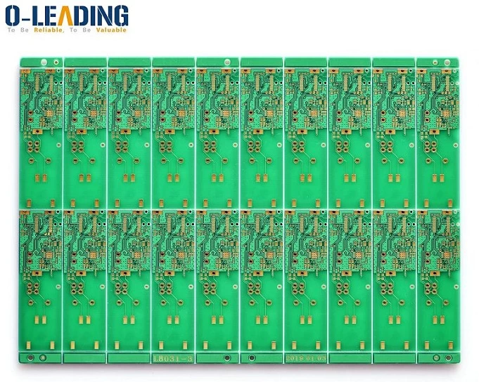
FR4 Rigid Double layer PCB manufacture China
Teardrop pads-often used when the traces connected to the pads are thin to prevent the pads from peeling and the traces from disconnecting the pads. Such pads are commonly used in high-frequency circuits.
Polygonal pads-used to distinguish pads with similar outer diameters and different apertures, which is convenient for processing and assembly.
Oval pad-This pad has enough area to enhance the peel resistance, and is often used in dual in-line devices.
Open pad-in order to ensure that after the wave soldering, the pad hole that is manually repaired is not sealed by the solder.
Two: Design standards for the shape and size of pads in PCB design
The minimum side of all pads is not less than 0.25mm, and the maximum diameter of the entire pad is not more than 3 times the component aperture.
Should try to ensure that the distance between the two pad edges is greater than 0.4mm.
In the case of dense wiring, it is recommended to use elliptical and oblong connection pads. The diameter or minimum width of the single-panel pad is 1.6mm; the weak-current line pad of the double-panel only needs to add 0.5mm in the hole diameter, and the excessively large pad can easily cause unnecessary continuous welding. The aperture exceeds 1.2mm or the pad diameter Pads over 3.0mm should be designed as diamond or plum-shaped pads.
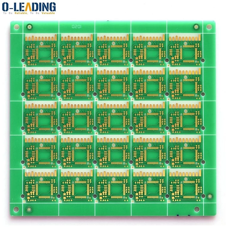
China OEM fast delivery 1 to 12 layers hasl FR4 electronic
For plug-in components, in order to avoid copper foil breakage during welding, the single-sided connection pad should be completely covered with copper foil; while the double-sided board needs at least tear drops.
All machine-inserted parts should be designed as dripping pads along the direction of the bent legs to ensure that the solder joints at the bent legs are full.
Large-area copper pads should use chrysanthemum-shaped pads, not to be soldered. If there is a large area of ground wire and power line area on the PCB (the area exceeds 500 square millimeters), it should be partially opened or designed as a grid fill.