


PCB design method for reducing multi-layer board to two-layer board
In the first step, in the layer definition under Setup, the layer definition of GND and VCC (Electrical Layer Type) is No Plane, OK to exit;
In the second step, delete all blind buried holes in the Pad Stacks under Setup and exit OK.
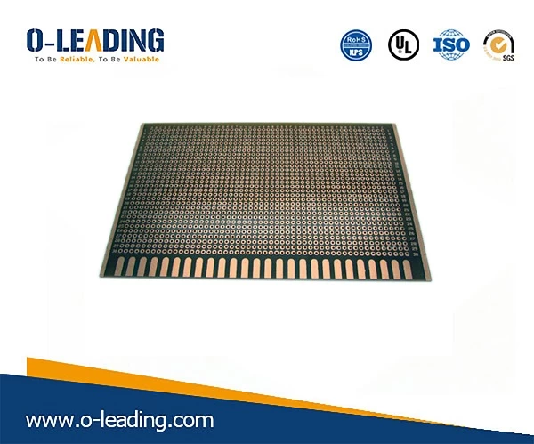
GLOBAL SUCCESS PCB supplier.
The third step is to close the top and bottom layers in the Display Colors under Setup, leaving only the middle two layers;
The fourth step is to enter the ECO mode;
The fifth step, right mouse button, Select Traces/Pins;
The sixth step, right mouse button, Select All;
In the seventh step, all the drilled pairs are deleted under the Drill pairs under setup;
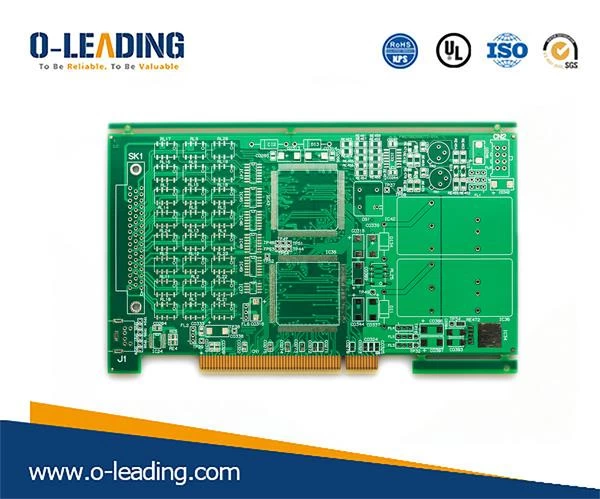
flexible BOARD manufacturer china.
In the eighth step, select Export under the menu bar File, save, click SELECT All in the ASCII OUTPUT dialog box, do not select PCB parameters;
Finally, the PCB design powerpcb builds a new file, and imports the file that just exists.
In addition, the 3.4 layer in the Reassign Electrical Layers in the board definition under Setup can be displayed as NO to be converted into two layers. If the display is YES, the network is not deleted.