PCB design - anti-interference
o-leading
o-leading.com
2018-07-31 14:12:24
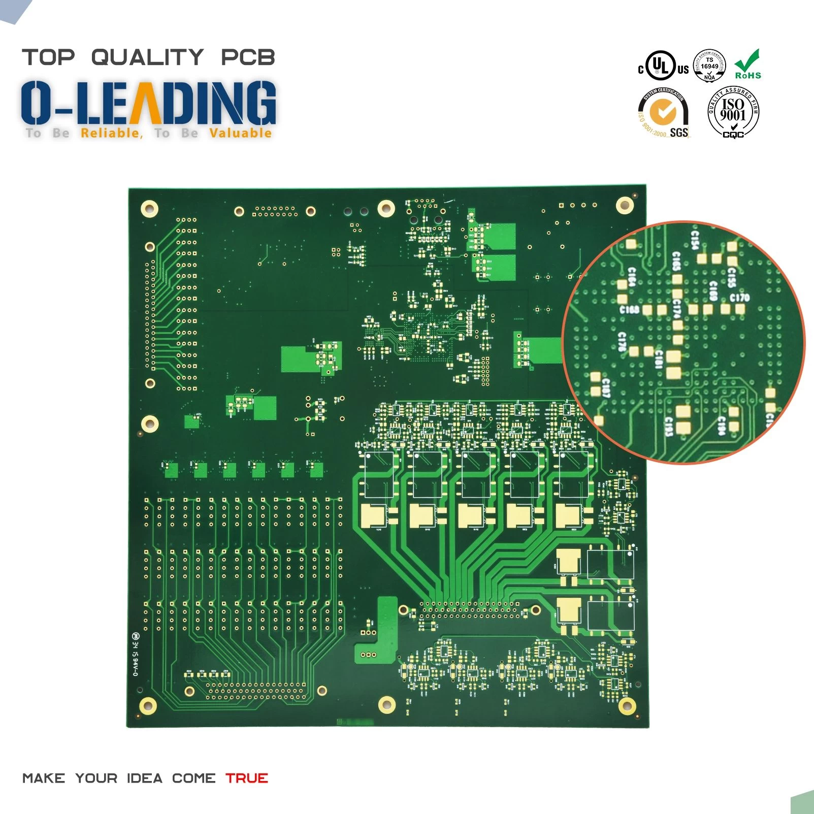
1. Power cord design. According to the current of the printed circuit board, try to increase the width of the power line and reduce the loop resistance. At the same time, the direction of the power line and the ground line is consistent with the direction of data transmission, which helps to enhance the anti-noise capability.(Printed circuit board supplier)
2. Lot design. The principle of ground design is: (1) The digital ground is separated from the simulated ground. If there are both logic and linear circuits on the board, they should be separated as much as possible. The ground of the low-frequency circuit should be grounded in parallel with a single point. If the actual wiring is difficult, it can be partially connected and then grounded in parallel. The high-frequency circuit should adopt multi-point series grounding, the ground wire should be short and rented, and the grid-like large-area foil should be used as much as possible around the high-frequency components. (2) The grounding wire should be as thick as possible. If the grounding wire uses a very strong line, the grounding potential changes with the change of the current, which reduces the noise immunity. Therefore, the ground wire should be thickened so that it can pass three times the allowable current on the printed board. If possible, the grounding wire should be 2~3mm or more. (3) The grounding wire constitutes a closed loop. In a printed circuit board composed only of digital circuits, the grounding circuit is mostly formed into a loop, which can improve the anti-noise capability.

3. Undo capacitor configuration. One of the usual practices in PCB design is to place appropriate untwisting capacitors at various critical points in the printed board.
4. Proper use of anti-interference devices. In the PCB electromagnetic compatibility design, the anti-interference device should be selected correctly according to the different characteristics of the noise. For example, diodes and varistors are used to absorb surge voltage, isolation transformers are used to isolate power supply noise, line filters are used to filter out interference signals in certain frequency bands, and combinations of resistors, capacitors, inductors, etc. are used to interfere with voltage or The current is bypassed, absorbed, isolated, filtered, decoupled, and the like. If the anti-interference device is not properly used, it will not effectively reduce the interference, and even become a new source of interference.


