


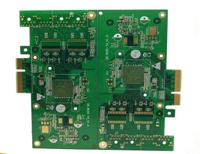
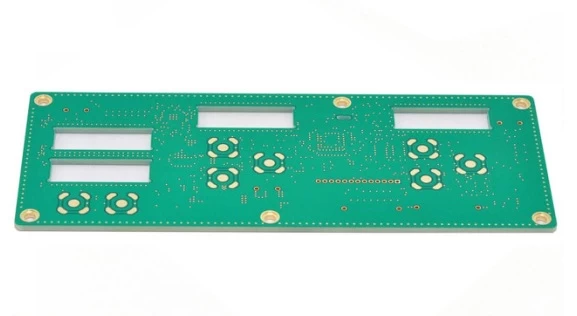
PCB negative VS positive
o-leading.com
o-leading.com
2017-08-30 14:04:05
The difference between PCB positive and negative:
PCB positive and negative effect is the final manufacturing process is the opposite.
PCB (Custom Circuit Boards china) positive effects: where the lines are drawn, the copper of the printing plate is retained, and where no lines are drawn, the copper is removed. Such as the top floor and the bottom floor... The signal layer is positive.
PCB (Printed circuit board in china) negative effect: any local copper printing plate of the line drawing is cleared, the local copper no painting line has been preserved. The Internal Planes layer (internal power / ground layer) (referred to as the inner layer) is used to arrange the power line and ground wire. Walk the line placed in these planes or other object is no copper area, namely the working layer is negative.
What are the benefits of an PCB (china pcb manufacturer) feature? What are the main features?
In order to reduce the negative is to reduce the amount of computation by file size. Where copper is not displayed, where no copper is displayed. This can significantly reduce the amount of data and computer display burden in the formation power layer. But now the computer configuration of this workload is be nothing difficult, I don't feel too negative recommendation, error prone. The pad is not well designed. It might be short circuited.
The power division is convenient, there are many methods, feature can also be very convenient power supply division in other ways, not necessarily negative.