


Common problems with RF circuits and digital circuits on the same PCB
The most sensitive node of an RF device is usually a loop-filtering circuit of a phase-locked loop (PLL), an external voltage-controlled oscillator (VCO) inductor, a crystal reference signal, and an antenna terminal. These parts of the circuit should be handled with special care.
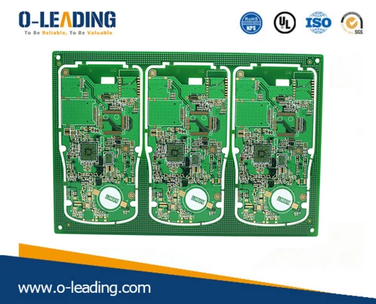
Telecommunication PCB supplier china.
(1) Power supply noise
Since the input/output signal has a swing of a few V, the digital circuit is generally acceptable for power supply noise (less than 50 mV). Analog circuits are quite sensitive to power supply noise, especially for glitch voltages and other high frequency harmonics.
Therefore, power line routing on PCB boards containing RF (or other analog) circuits must be more careful than wiring on a common digital board, and automatic routing should be avoided. It should also be noted that the microcontroller (or other digital circuit) will suddenly draw most of the current for a short period of time within each internal clock cycle, since modern microcontrollers are designed in a CMOS process.
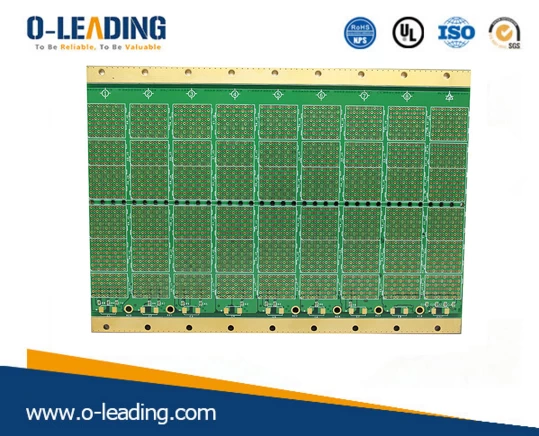
Immersion Gold PCB in china.
Therefore, assuming that a microcontroller is operating at an internal clock frequency of 1 MHz, it will draw (pulse) current from the supply at this frequency. If no proper power supply decoupling is used, it will cause voltage spikes on the power line. If these voltage spurs reach the power supply pin of the RF portion of the circuit, serious operation can be caused, so the analog power supply line must be separated from the digital circuit area.
(2) Unreasonable ground wire
The RF board should always be routed with a ground plane connected to the negative side of the power supply, which can cause some strange behavior if not handled properly. This may be difficult for a digital circuit designer to understand because most digital circuit functions perform well even without a ground plane. In the RF band, even a short line will act like an inductor. Rough calculation, the inductance per mm length of about 1 nH, the inductance 434 MHz 10 mmPCB line is approximately 27 Ω. If the ground plane is not used, most of the ground will be longer and the circuit will not guarantee design features.
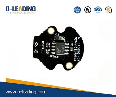
Golden Fingers PCB manufacturer china.
(3) Radiation of the antenna to other analog parts
This is often overlooked in circuits that contain RF and other parts. In addition to the RF section, there are usually other analog circuits on the board. For example, many microcontrollers have built-in analog-to-digital converters (ADCs) for measuring analog inputs as well as battery voltage or other parameters.
If the antenna of the RF transmitter is located near this PCB (or just on this PCB), the high frequency signal that is sent may reach the analog input of the ADC. Don't forget that any circuit line can emit or receive RF signals like an antenna. If the ADC input is not handled properly, the RF signal may self-excite in the ESD diode of the ADC input, causing ADC bias.