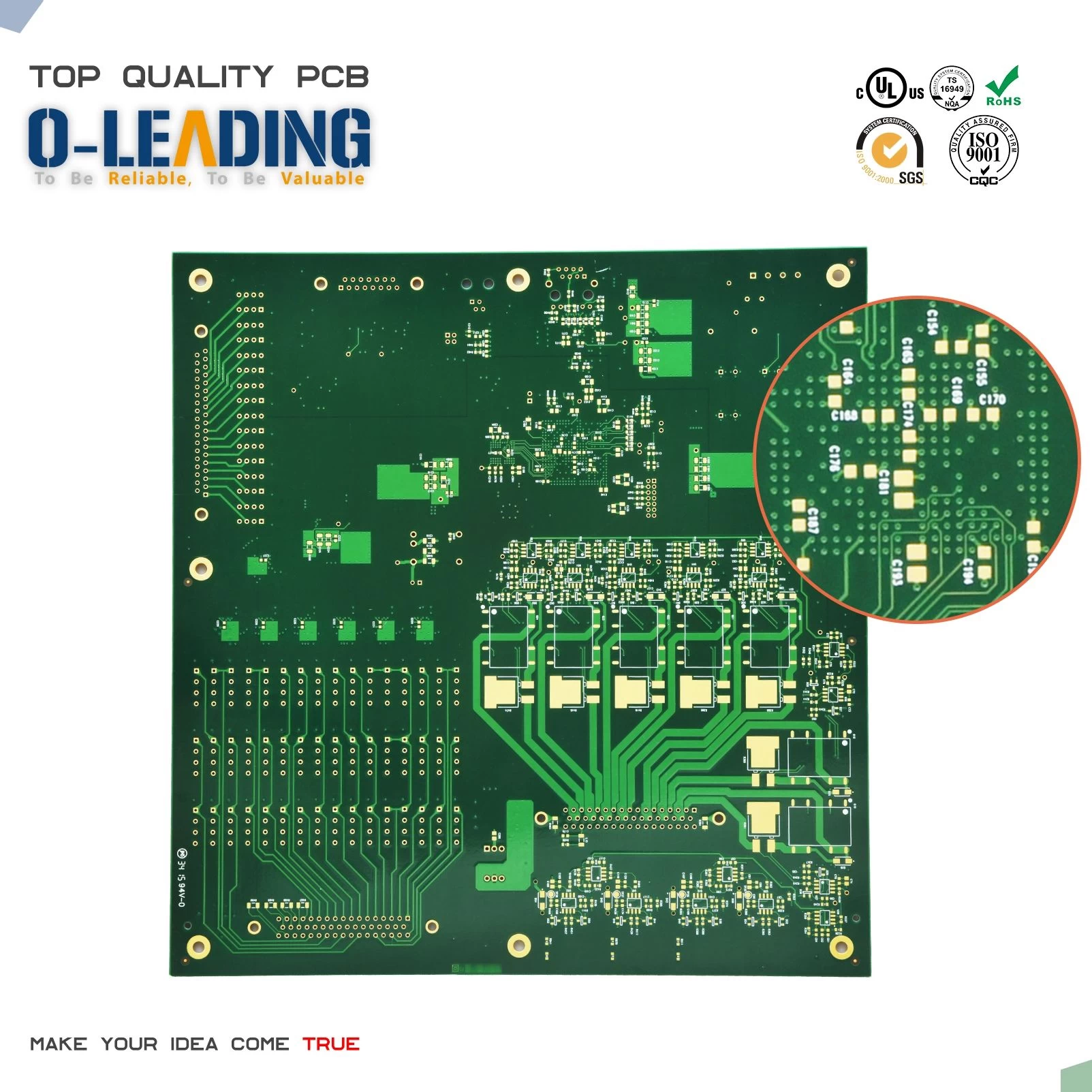
Can pcb layout be routed at 90°?
Of course, when the signal propagates along a uniform interconnect, there will be no distortion of the reflected and transmitted signals. If there is a 90° corner on the uniform interconnect, it will cause a change in the width of the pcb transmission line at the corner, according to the correlation. Electromagnetic theory calculates that this will definitely bring about the reflection of the signal.
For example, Wang Decong students (here Wang’s classmates are purely old wu for the plot needs to be fictional, and certainly no biological father will take such a name for his son. If there is similarity, it is purely an honor. Take the second ha and the female ticket of their family to go to the hot pot and see that the roadside has lost a hundred dollars. Do you say that he is still not?
Picking up this hundred pieces, in theory, Wang Decong’s personal wealth has increased by another hundred, but for Wang’s classmates who are looking for a female to buy a luxury car, such as cabbage, can be completely ignored. For the old wu, this is a huge amount of money, I usually rush to pretend to tie the laces...
SMD stencil manufacturer china.
Therefore, the 90° corner has a negative impact on the high-speed signal transmission line, which is theoretically certain, but is this effect fatal? Is the 90° corner the same for high-speed digital signals and high-frequency microwave signal transmission lines?
For high-speed digital signals, the 90° corner will have a certain impact on the high-speed signal transmission line. For our high-density high-speed pcb, the general trace width is 4-5mil, and the capacitance of a 90° corner is about 10fF. It is estimated that the delay caused by this capacitor is increased by about 0.25 ps. Therefore, the 90° corner on the 5 mil line width wire does not greatly affect the current high speed digital signal (100-psec rising edge time).
Global circuits supplier china.
For high-frequency signal transmission lines, in order to avoid signal damage caused by the skin effect, a wider signal transmission line is usually used, for example, 50Ω impedance, 100mil line width, and the line width at the 90° corner is about At 141mil, the signal delay caused by parasitic capacitance is about 25ps. At this time, the 90° corner will have a very serious impact.
At the same time, the microwave transmission line always hopes to minimize the loss of the signal. The impedance discontinuity at the 90° corner and the parasitic capacitance outside will cause the phase and amplitude errors of the high frequency signal, the mismatch of the input and output, and possible Parasitic coupling, which in turn leads to deterioration of circuit performance and affects the transmission characteristics of PCB circuit signals.

