


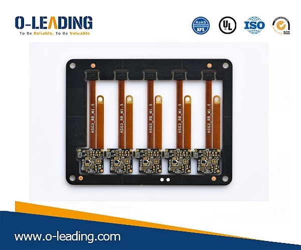
PCB wiring these several ways, can you?
In the process of learning embedded development, PCB layout is essential. A good wiring method looks beautiful and has a reasonable layout in the light, and can save production costs in the light of it, achieve good circuit performance and heat dissipation performance, and optimize the performance of components. Today, Xiaobian sorted out the common wiring methods in PCB design, I hope everyone can be inspired after reading.
Clock wiring
The clock line is one of the factors that has the biggest impact on EMC. There should be fewer holes in the clock line, try to avoid running parallel to other signal lines, and keep away from general signal lines to avoid interference with signal lines. At the same time, avoid the power part of the board to prevent the power and clock from interfering with each other.
If there is a dedicated clock generator chip on the board, no traces can be routed under it. Copper should be laid underneath it, and if necessary, it can also be dedicated to ground. For many chips, there are reference crystal oscillators, and there should be no traces under these crystal oscillators. Copper isolation should be used.
Trace angle
Right-angle wiring is generally a situation that PCB wiring requires to be avoided as much as possible, and it has almost become one of the standards for measuring the quality of the wiring. So how much influence does right-angle wiring have on signal transmission?
In principle, running at right angles will change the line width of the transmission line, causing discontinuities in impedance. In fact, whether it is a right-angle line, a bevel angle, or an acute-angle line, the impedance may change.
The impact of a right-angle trace on the signal is mainly reflected in three aspects: first, the corner can be equivalent to a capacitive load on the transmission line, which slows down the rise time; second, the impedance discontinuity will cause signal reflection; third, the right-angle tip produces EMI.
Differential trace
Compared with ordinary single-ended signal traces, the most obvious advantages of differential signals are reflected in the following three aspects:
Strong anti-interference ability, because the coupling between the two differential traces is very good. When there is noise interference from the outside, it is almost coupled to the two lines at the same time, and the receiver only cares about the difference between the two signals. The common-mode noise can be completely canceled.
Can effectively suppress EMI. For the same reason, because the two signals have opposite polarities, the electromagnetic fields radiated by them can cancel each other out. The tighter the coupling, the less electromagnetic energy is released to the outside.
Timing positioning is accurate. Because the switching change of the differential signal is located at the intersection of the two signals, unlike ordinary single-ended signals, which rely on two threshold voltages for judgment, it is less affected by process and temperature, which can reduce timing errors. It is also more suitable for circuits with low amplitude signals.
Serpentine
Serpentine is a type of routing method often used in layouts. Its main purpose is to adjust the delay and meet the system timing design requirements. The designer must first have this understanding: the serpentine line will destroy the signal quality, change the transmission delay, and try to avoid it when wiring. However, in actual design, in order to ensure that the signal has sufficient holding time, or to reduce the time offset between the same group of signals, it is often necessary to deliberately perform winding.
Conclusion: When we design differential signal lines that appear in pairs, we usually run them in parallel to minimize the number of holes. When a hole must be punched, the two wires should be punched together to achieve impedance matching. A group of buses with the same properties should be routed side by side as far as possible, so as to be as long as possible, and the vias from the pads should be as far away from the pads as possible. In short, when learning PCB wiring, while we have mastered some rules, it is more important to be able to design more hands-on and use data to calculate the best results.