


Analysis of failure of electronic components
To carry out failure analysis of electronic components, some advanced analytical testing techniques and instruments are needed.
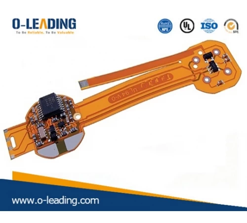
flexible BOARD manufacturer china
1 optical microscope analysis technology
Optical microscope analysis techniques mainly include stereo microscopes and metallographic microscopes.
The stereo microscope has a small magnification, but the depth of field is large; the magnification of the metallographic microscope is large, from several tens of times to more than one thousand times, but the depth of field is small. Using these two microscopes together, the appearance of the device, as well as the surface shape, distribution, size, organization, structure and stress of the failure site, can be observed. For example, it is used to observe the burnout and breakdown of the chip, wire bonding, substrate cracks, contamination, scratches, oxide layer defects, corrosion of the metal layer, and the like. The microscope can also be equipped with auxiliary devices that provide viewing methods such as brightfield, darkfield, differential interference phase contrast, and polarization to suit various needs.
2 infrared analysis technology
The structure of the infrared microscope is similar to that of a metallographic microscope. However, it uses a near-infrared (wavelength of 0175~3 micron) light source and is imaged by an infrared image tube. Semiconductor materials such as germanium and silicon and thin metal layers are transparent to infrared radiation. With it, the chip without cutting the device can also observe defects and soldering conditions inside the chip. It is also particularly suitable for failure analysis of plastic packaged semiconductor devices.
Infrared microscopy is a method for high-precision non-contact temperature measurement of tiny areas of microelectronic devices using infrared microscopy. The operation and failure of the device is reflected by thermal effects. Improper device design, material defects, process errors, etc. will cause local temperature rise. Hot spots may be as small as microns, so temperature measurement must be for small areas. In order not to affect the operation and electrical characteristics of the device, the measurement must be non-contact. Finding hot spots and measuring the temperature with high precision in a non-contact manner is of great significance to product design, process control, failure analysis, and reliability inspection.
The infrared camera is a non-contact temperature measurement technology that measures the temperature at each point on the surface and gives the temperature distribution on the surface of the sample.
The infrared camera scans the sample at high speed with an optical system such as a vibration or a mirror, and condenses the heat radiation from each point on the surface of the sample onto the detector to become an electrical signal, and then the display forms a black-and-white or color image. Used to analyze the temperature at various points on the surface.
3 acoustic microscopy analysis
Ultrasound can be transmitted in homogeneous materials such as metals, ceramics and plastics. Ultrasonic inspection of the surface and underside of the material can detect macroscopic defects such as multilayer structural integrity. Ultrasound is a very effective means of detecting defects and performing failure analysis. Combining ultrasonic testing with advanced light, machine and electrical technologies, it also develops acoustic microscopic analysis technology, which can be used to observe the internal conditions of samples that cannot be seen by optical microscopes, and can provide high contrast that cannot be obtained by X-ray fluoroscopy. Images can be applied to non-destructive analysis.
4 liquid crystal hot spot detection technology
As mentioned above, hot spot detection is an effective means in semiconductor device failure analysis.
Liquid crystal is a liquid, but when the temperature is lower than the phase transition temperature, it becomes a crystal.
The crystal will show anisotropy. When it is heated and the temperature is higher than the phase transition temperature, it becomes an isotropic liquid. Using this property, it is possible to observe the phase transition point of the liquid crystal under orthogonally polarized light to find a hot spot.
The liquid crystal hot spot detecting device is composed of a polarizing microscope, an adjustable temperature sample stage, and an electric bias control circuit of the sample.
Liquid crystal hot spot detection technology can be used to check for defects such as pinholes and hot spots. If a pinhole exists in the oxide layer, the metal layer above it and the underlying semiconductor may be short-circuited, causing deterioration or even failure of electrical characteristics. Apply the liquid crystal to the surface of the tube to be tested, and then place the sample on the heating stage. If the oxide layer of the tube has pinholes, leakage current will occur and heat will be generated, so that the temperature rises at this point, and the polarized light is used. Under the optical microscope, the difference between the hot spot and the surrounding color can be observed to determine the location of the hot spot on the device.
Due to the low power consumption, this method has high sensitivity and high spatial resolution.
5 optical radiation microscopy technology
When a semiconductor material is excited by an electric field, carriers will transition between energy levels to emit photons. The optical radiation in semiconductor devices and integrated circuits can be divided into three categories: one is the composite radiation in which the minority is injected into the pn junction, that is, the unbalanced minority carriers are injected into the barrier and combined with the majority carriers to emit photons. Second, the electric field accelerates the luminescence of the carrier, that is, the high-speed moving carriers generated under the action of the strong electric field collide with the atoms on the lattice to make them ionize and emit light. The third is the medium of light. Under a strong electric field, when a tunnel current flows through a dielectric film such as silicon dioxide or silicon nitride, photon emission occurs.
The light-radiation microscope uses a low-light detection technique to increase the photon detection sensitivity by six orders of magnitude, combined with digital image technology to improve the signal-to-noise ratio.
After the 1990s, the function of spectral analysis of the detected optical radiation was added to determine the type and nature of the optical radiation.
To perform optical radiation microscopy, firstly, a real-time image detection of the sample is performed under an external light source, and then a bias is applied to the portion to detect the optical radiation of the sample in an opaque shielding box.
In a semiconductor device, various types of defects and damages may generate electric leakage under the action of a certain intensity electric field, and accompany the jump of the carriers to generate optical radiation, so that the positioning of the light-emitting portion may be the positioning of the failed portion. At present, the types of defects and damages that can be detected by optical radiation microscopy techniques include leakage junctions, contact spikes, oxidation defects, gate pinholes, electrostatic discharge damage, latch-up effects, hot carriers, saturated transistors, and switching transistors. and many more.
6 microanalysis technology
Microanalysis is a technique for in-depth analysis of electronic components. The failure of components is directly related to the chemical composition of the materials used, the structure of the devices, and the morphology of the microdomains. Failure is also related to many factors such as fluctuations and precision of process control, material stability, and physical and chemical properties of various materials. In order to deeply understand and study the causes, mechanisms and modes of failure, in addition to the above-mentioned techniques, it is necessary to clarify the relevant micro-areas and obtain informative information.
With the diversification of materials used in components, the complexity and refinement of the process, and the miniaturization of the dimensions, the requirements for microanalysis are becoming more and more urgent. This technology has been widely used abroad for reliability and failure analysis. Since the reform and opening up, China has introduced a large number of large-scale analytical test instruments, and it has fully met the conditions for conducting micro-analysis.
Microanalysis technology uses electrons, ions, photons, laser beams, X) rays and nuclear radiation to act on the sample to be analyzed, and excites the sample to emit electrons, ions, photons, etc., and uses sophisticated instruments to measure their energy, intensity, and Information such as spatial distribution is used to analyze the composition, structure, and the like of the sample.
The first step in the microanalysis work is to look at the shape and look at the device's graphics, linework, and misalignment. Scanning electron microscopy (SEM) and transmission electron microscopy (STM) can be used to observe this. STM can be amplified by hundreds of thousands of times and can almost resolve atoms.
In order to understand the materials used to make the components, they can be detected by instruments such as Auger electron spectroscopy (AES), secondary ion mass spectrometry (SIMS) and X-ray photoelectron spectroscopy (XPS). It is also possible to use the X-ray energy spectrum or spectrum attached to the SEM and STM for composition analysis. AES also gives the distribution of components on the surface. In order to understand the depth distribution of the components, instruments such as AES and XPS also have ion guns, and the components are tested by ion etching to know how the components are distributed according to depth. In order to obtain higher lateral resolution, the AES test, the focal spot of the electron beam should be small, and the XPS of the small spot should be used.
Materials used in electronic components range from light elements to heavy elements such as gold, platinum and tungsten. Different instruments are often used to detect different elements. When using AES to detect light elements, it is less sensitive.
An important aspect of device detection is the analysis of the crystal structure of the film and substrate, including understanding the crystal orientation of the substrate, detecting whether the film is single crystal or polycrystalline, the preferred orientation of the polycrystal, the grain size, the stress of the film, etc. This information is mainly obtained by X-ray diffraction (XRD) instrument. The target X-ray diffractometer emits a strong X-ray, which is a very sensitive instrument for structural detection. SEM and STM can also obtain information about the crystal structure while observing the morphology, such as observing the grain of the film. It can also be used for electron diffraction on STM, which is more sensitive than ordinary X-ray diffraction.
o-leading.
You can contact sales@o-leading.com
As a part of our constant efforts toward improvement, we welcome your feedback.
O-leading is all about delivering your printed circuit boards and assemblies on time, and providing excellent quality.
We appreciate your business, and look forward to serving you.