


- Kontaktiere uns
-
TEL: + 86-13428967267
FAX: + 86-4008892163-239121
+ 86-2028819702-239121
E-Mail: sales@o-leading.com
 Kontaktieren Sie mich jetzt
- Zertifizierungen
-


- Abonnieren
-
Erhalten Sie E-Mail-Updates zu neuen Produkten
- Neue Produkte


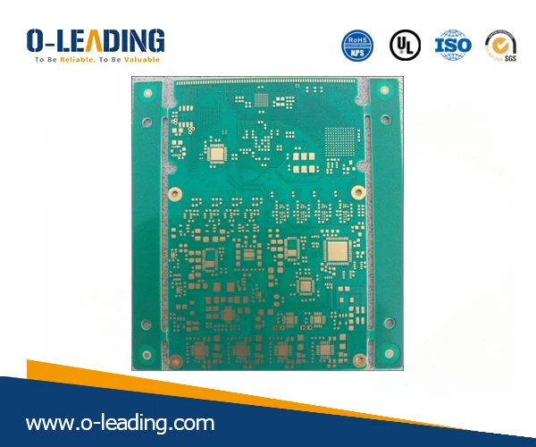
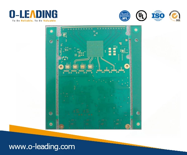
Bare printed circuit board company, High Quality PCBs china
- Product Nature
- Layer count: 10L 2+(6)+2
- materials: Megtron 6
- Board thickness: 1.6+/-0.16mm
- Surface finish: ENIG
- Special : 10% impedance, 8mil laser drill, POFV, stacked via, laser blind via drill thru 6mil dielectric and plug and plating flat via
- Application: 100G CFP (Optical module)
COPPER PLATE HOLES MINIMUM .025 AVG, .020 MIN.. HOLES MAY NOT BE PLUGGED
This PN required 10% impedance, 8mil laser drill, POFV, stacked via, laser blind via drill thru 6mil dielectric and plug and plating flat via
Pack with colorless transparent bubble film ,25 PCS/ bag, put desiccant in flank, put humidity indicator card on top side
Layer structure
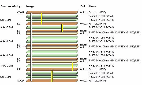
This PN required 10% impedance, 8mil laser drill, POFV, stacked via, laser blind via drill thru 6mil dielectric and plug and plating flat via
Pack with colorless transparent bubble film ,25 PCS/ bag, put desiccant in flank, put humidity indicator card on top side
Layer structure
- Andere Produkte

, Hochfrequenz PCB, Immersion AG, Blind/vergraben über Löcher Hersteller")