


- Свяжитесь с нами
-
ТЕЛ: + 86-13428967267
ФАКС: + 86-4008892163-239121
+ 86-2028819702-239121
Электронная почта: sales@o-leading.com
 Связаться сейчас
- Сертификация
-


- Подписаться
-
Получайте обновления по электронной почте о новых продуктах


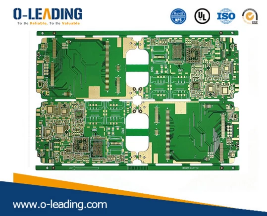
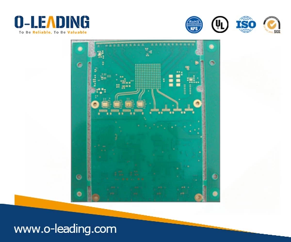
Printed Circuit Board PCB Manufacturing Company, Pcb prototype manufacturer china
- Product Nature
- Layer count: 10L 2+(6)+2
- materials: Megtron 6
- Board thickness: 1.6+/-0.16mm
- Surface finish: ENIG
- Special : 10% impedance, 8mil laser drill, POFV, stacked via, laser blind via drill thru 6mil dielectric and plug and plating flat via
- Application: 100G CFP (Optical module)
COPPER PLATE HOLES MINIMUM .025 AVG, .020 MIN.. HOLES MAY NOT BE PLUGGED
This PN required 10% impedance, 8mil laser drill, POFV, stacked via, laser blind via drill thru 6mil dielectric and plug and plating flat via
Pack with colorless transparent bubble film ,25 PCS/ bag, put desiccant in flank, put humidity indicator card on top side
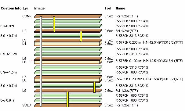
Layer structure

This PN required 10% impedance, 8mil laser drill, POFV, stacked via, laser blind via drill thru 6mil dielectric and plug and plating flat via
Pack with colorless transparent bubble film ,25 PCS/ bag, put desiccant in flank, put humidity indicator card on top side
Layer structure
Тег:
- Другие продукты

, высокочастотная ПХД, АГ, слепая/захороненная через отверстия производителя")