


What is the role of each layer in the PCB board, and what should I pay attention to when using it?
1.Mechanical mechanical layer, as the name implies, is the appearance of the entire PCB board for mechanical shaping. In fact, when we say the mechanical layer, we mean the overall structure of the PCB board. It can also be used to set the board dimensions, data marks, alignment marks, assembly instructions, and other mechanical information. This information varies depending on the requirements of the design company or PCB manufacturer. In addition, the mechanical layer can be attached to other layers and output and displayed together.
2. Keep out layer (forbid wiring layer), used to define the area where components and wiring can be effectively placed on the circuit board. Draw a closed area on this layer as the effective area for routing. Outside this area, you cannot automatically place and route. The wiring forbidden layer defines the boundary when we lay copper with electrical characteristics. That is to say, after we define the wiring forbidden layer, it is impossible for us to lay wires with electrical characteristics in the subsequent wiring process. The boundary of the layer is often used to use the Keepout layer as a mechanical layer. This method is actually wrong, so it is recommended that you distinguish them, otherwise the board factory will give you attribute changes every time it is produced.
3.Signal layer: The signal layer is mainly used to arrange the wires on the circuit board. Including Top layer (bottom layer), Bottom layer (bottom layer) and 30 MidLayer (middle layer). The top and bottom layers place devices, and the inner layers are routed.
4. Top paste and Bottom paste are the top and bottom pad stencil layers, which are the same size as the pads. This is mainly when we are doing SMT, we can use these two layers to make the stencil. Just digging a pad-sized hole on the Internet, we then covered this steel mesh on the PCB, and brushed it with a brush with solder paste evenly.
5. Top Solder and Bottom Solder This is a solder mask that prevents green oil from covering. We often say "opening the window". Conventional copper or traces are covered by green oil by default. If we correspondingly solder the mask If it is processed, it will prevent the green oil from covering and will expose the copper.
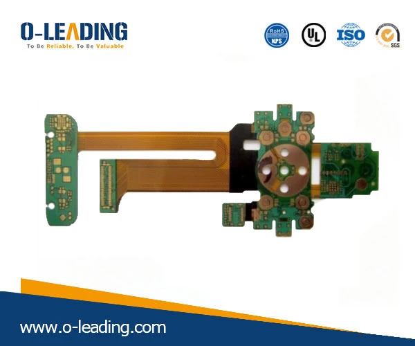
Multiple Flex-Rigid Board factory
6.Internal plane layer (internal power / ground layer): This type of layer is only used for multi-layer boards, which are mainly used to arrange power lines and ground lines. We call double-layer boards, four-layer boards, and six-layer boards. Number of signal layers and internal power / ground layers.
7.Silkscreen layer: The silkscreen layer is mainly used to place printed information, such as the outline and annotation of components, various comment characters, etc. Altium provides two screen printing layers, Top Overlay and Bottom Overlay, which place the top screen printing file and the bottom screen printing file respectively.
Screen Printing Bending Ink wholesales
8. Multi layer: The pads and penetrating vias on the circuit board must penetrate the entire circuit board and establish electrical connections with different conductive pattern layers. Therefore, the system specifically sets an abstract layer—multi-layer . Generally, the pads and vias must be set on multiple layers. If this layer is closed, the pads and vias cannot be displayed.
9.Drilling Layer: The drilling layer provides drilling information during the manufacturing of the circuit board (such as pads, vias, etc.).