


The 8 classic problems of PCB (Part 2)
Question 5: PCB open circuit
An open circuit occurs when the trace is broken, or when the solder is only on the pad and not on the component lead. In this case, there is no adhesion or connection between the component and the PCB. Just like short circuits, these can also occur during production or welding and other operations. Vibrating or stretching the circuit board, dropping them, or other mechanical deformation factors can damage traces or solder joints. Similarly, chemicals or moisture can cause solder or metal parts to wear, which can lead to breakage of component leads.
Question 6: Loose or misaligned components
During reflow soldering, small parts may float on the molten solder and eventually break away from the target solder joint. Possible causes of displacement or tilt include vibration or bounce of components on the soldered PCB due to insufficient circuit board support, reflow oven settings, solder paste problems, human error, etc.
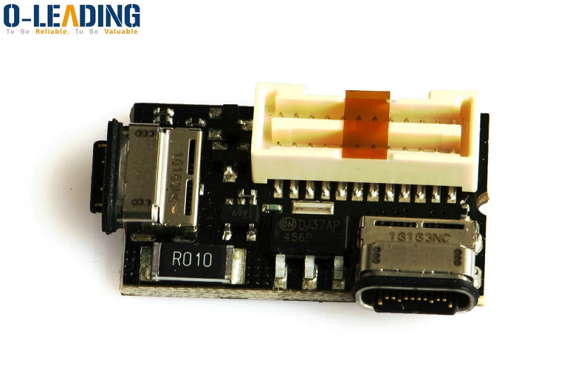
Original Electronic pcb and pcba wifi remote control circuit board fabrication
Question 7: Welding issues
The following are some of the problems caused by poor welding practices:
Disturbed solder joints: Solder moves before solidification due to external disturbances. This is similar to cold solder joints, but for different reasons, it can be corrected by reheating, and to ensure that the solder joints are not interfered by the outside when they are cooled.
Cold soldering: This situation occurs when the solder cannot be melted correctly, resulting in rough surfaces and unreliable connections. Since excess solder prevents complete melting, cold solder joints may also occur. The remedy is to reheat the joint and remove excess solder.
Solder bridge: This happens when the solder crosses and physically connects the two leads together. These may form unexpected connections and short circuits, which may cause the component to burn out or blow the trace when the current is too high.
Pad: Inadequate wetting of leads or leads. Too much or too little solder. Pads that are elevated due to overheating or rough soldering.
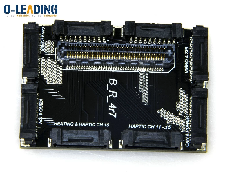
Printed circuit board manufacturer China
Question 8: Human error
Most of the defects in PCB manufacturing are caused by human errors. In most cases, incorrect production processes, incorrect placement of components, and unprofessional manufacturing specifications are responsible for up to 64% of avoidable product defects. Due to the following points, the possibility of defects increases with the complexity of the circuit and the number of production processes: densely packaged components; multiple circuit layers; fine wiring; surface soldered components; power supply and ground plane.
Although every manufacturer or assembler hopes to produce a PCB board without defects, it is because there are several kinds of difficulties in the design and production process that have caused PCB board problems.
Typical problems and results include the following: poor soldering can cause short circuits, open circuits, cold solder joints, etc.; misalignment of the layers can cause poor contact and poor overall performance; poor insulation of copper traces can cause traces and traces An arc occurs between the wires; the copper traces are too tightly connected to the vias, which is prone to the risk of short circuit; insufficient circuit board thickness can lead to bending and breaking.