


- Contact Us
-
TEL: + 86-13428967267
FAX: + 86-4008892163-239121
+ 86-2028819702-239121
Email: sales@o-leading.com Contact Now
- Certifications
-


- Subscribe
-
Get email updates on new products
- New Products


- Electronic album


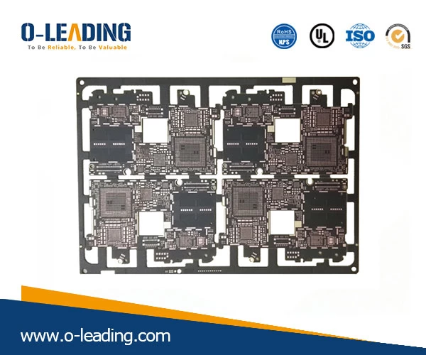

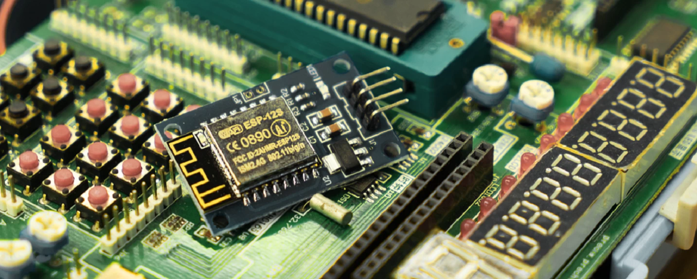
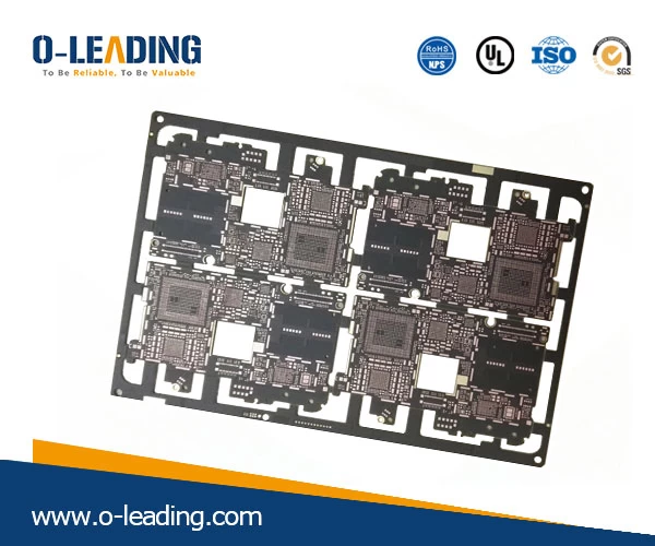
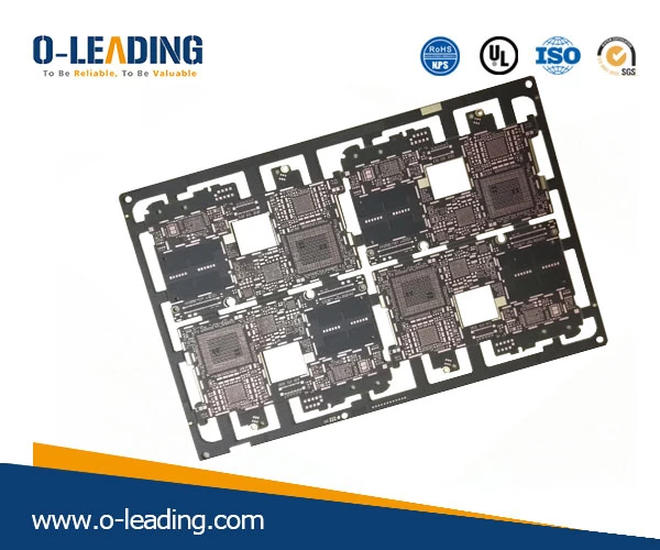
HDI pcb Printed circuit board, led pcb board manufacturer
- PCB P / N: 1045633
- Number of layers: 12L
- Material: EM-370(5) Mid-TG
- Board THK: 0.85+/-10% mm
- Copper thk: 1 1oz
- The smallest hole size: 0.1 mm
- Number of holes (pcs.): 980
- Line w / s: 2.4/2.4mil
- Impedance control. Y / N (Tol%): N
- Surface treatment: ENIG+OSP
- Mask for solder Silkscreen: Green
- The size of one board: Dim X (mm): 43.2; Dim Y (mm): 62.1
- Panelisation: Dim X (mm): 98.4; Dim Y (mm): 140.2; No UPS: 4
- Specially: flaking mask: N
- Routing / Perforation: CNC
|
Place of origin |
Guangdong China (Mainland) |
Brand name |
O-Leading |
|
Basic Material |
EM-370(5) Mid-TG |
Copper thickness |
1oz |
|
Minimum Hole Size |
0.1mm |
Minimum Line width |
0.2mm |
|
Surface treatment |
Immersion gold, OSP |
Plate thickness |
0.1-5mm |
|
Applicable to |
Lead, mobile phone, air Air conditioners, washing machines |
character |
Industrial controller |
|
Certificates |
ISO9001, UL, RoHS, SGS |
Q / CTN |
10pcs-100pcs |
|
the weight |
0.01kg-5kg |
MOQ |
10 pieces |
| Model number | Assembling the power bank pcb pcba manufacturer | Minimum Line spacing | 0.2mm |
| Colour | black | price | $ 0.1- $ 10 |
| Type desigh | Customer requirement | the size | 0.01m3-10m3 |
Packing & Delivery
|
Packaging Details |
16-year-old professional OEM client Board Manufacturer |
|
Delivery detail |
7-12days. |
Packing & Delivery
Packaging Details: 16-year-old professional OEM client Board Manufacturer
Delivery detail: 7-12days.
|
paragraph |
2017 |
2018 ~ 2020 |
2021 ~ 2023 |
|||
|
Amount |
Sample |
Amount |
Sample |
Amount |
Sample |
|
|
Number of layers |
32 |
42 |
38 |
44 |
42 |
48 |
|
Min. Line / Spacing (μm) |
50/50 |
40/45 |
40/45 |
40/40 |
35/40 |
35/35 |
|
Min. Drilling hole |
0,15 |
0.10 |
0,15 |
0.10 |
0,15 |
0.10 |
|
Aspect Ratio |
14: 1 |
16: 1 |
16: 1 |
18: 1 |
18: 1 |
20: 1 |
|
N + C + N, |
4 + C + 4 |
5 + C + 5 |
5 + C + 5 |
6 + C + 6 |
5 + C + 5 |
6 + C + 6 |
|
Any layer Relationship |
5 + 2 + 5 |
6 + 2 + 6 |
5 + 2 + 5 |
6 + 2 + 6 |
5 + 2 + 5 |
6 + 2 + 6 |
|
Filling of plates through |
YES |
- |
YES |
- |
YES |
- |
|
Minimum Core Thickness (Excluding copper) (μm) |
50 |
40 |
40 |
thirty |
40 |
thirty |
|
Minimum Laser Drill Diameter (μm) |
75 |
65 |
65 |
50 |
50 |
40 |
|
Via at the Funeral |
YES |
- |
YES |
- |
YES |
- |
|
material |
FR4, Megtron, Nelco, Rogers, Heavy Copper, etc. |
|||||
|
Built-in capacitor printed circuit board
|
YES |
- |
YES |
- |
YES |
- |
|
Surface process |
Lead-free HASL, ENIG, OSP, silver with immersion, tin of immersion, |
|||||

- Other Products


