


Printed Circuit Board Production Process
o-leading.com
o-leading.com
2017-03-23 15:50:21
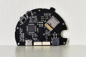
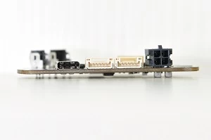
A self consisted of component of interconnected electronic elements develops a Printed. PCBs or printed are created with the help of a slim layer of carrying out material, either published on the surface area board, or performing material. And a PCB produced with booming digital parts is called a printed circuit setting up (PCBA).
High quality pcb manufacturer requires to adhere to a details treatment, remembering all the min details of its design. To execute the production of board, you should adhere to some actions. Following are some steps called for in Circuit Board Production:
1. Arrangement - The process of Motherboard Manufacturing could conveniently take a toll from you, otherwise done properly. So, you need to deal with some standard points like process, material needed, consumer requirements, and also most importantly customer's contentment.
2. Pattern|Etching - Etching does not literally mean inscription, yet has to do something with it. In this, copper as well as various other unguarded areas are revealed by the etch withstand film to get rid of the unsafe copper. This leaves the secured copper pads and also traces in position. Nonetheless, sophisticated as well as newer processed use plasma or laser etching as opposed to using chemicals for Circuit card Manufacturing.
3. Engraving photos - In this, a photo mask is combined with chemical etching in order to subtract the copper areas from the printed boards.
4. Multilayer Pushing - Among one of the most important action in PCB Manufacturing. This entails aligning of conductive copper and protecting di-electric layers. This is done to create a solid board product.
5. Boring - Quite plainly, this involves exploration of openings as well as the info gets on kept on the location, where the opening is intended to be pierced.
6. Masking - A safety layer is used over the copper, which has a thin layer of solder mask as well as copper traces around it. This is called concealing.
7. Finishing - In this, the pad areas are coated with a slim solder layer. This is carried out in order to prepare the board for wave soldering.
8. Electric Checking - This is the final blow where you are recommended to inspect the connection or shorted PCB Production links. To do this, you have to use voltage between the points.