


Laser marking technology helps to trace the information of PCB boar
o-leading
o-leading.com
2018-07-13 10:59:03
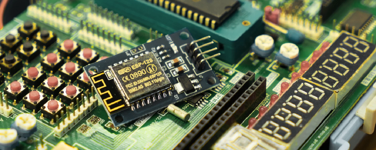
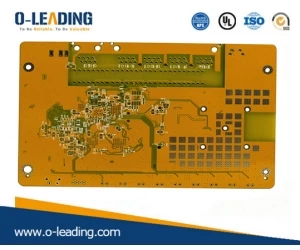
At present, PCB marking processing mainly has two methods: silk screen printing and laser marking.
The traditional silk screen processing uses a well-made graphic screen to transmit the character ink from a part of the mesh of the screen and leaks on the surface of the board by external pressure. The rest of the mesh on the screen will be blocked, not through the ink, only blank on the surface of the board, the ink under the leak will form the text, logo, pattern and so on. This kind of processing method is relatively cheap and the processing speed is fast, but there are shortcomings such as rough marking effect, easy to fall off the logo, unable to mark the PCB board (pcb manufacturer in china)with small web surface, and certain toxicity of chemical raw materials.
Laser marking uses a high-energy-density laser to locally illuminate the PCB, causing the surface material to vaporize or discolor, leaving a permanent mark. This non-contact processing marks very clear two-dimensional codes on very small webs, ensuring high precision while ensuring high quality without wear and tear due to high and low temperature, acid and alkali changes and external friction. No chemical assistance is required, and there is no negative effect on personnel safety and environment.
The dedicated laser marking machine for PCBs can compensate for the shortcomings of silk screen processing with its precision and flexibility, greatly improving production efficiency and yield, reducing costs and reducing pollution. Laser marking is becoming the best way to mark PCBs, and has been widely used in many fields such as digital products, wearable devices, and automotive circuit boards.