


The Design And Operation Procedure Of Double-Layer PCB
o-leading.com
o-leading.com
2017-12-13 11:43:40
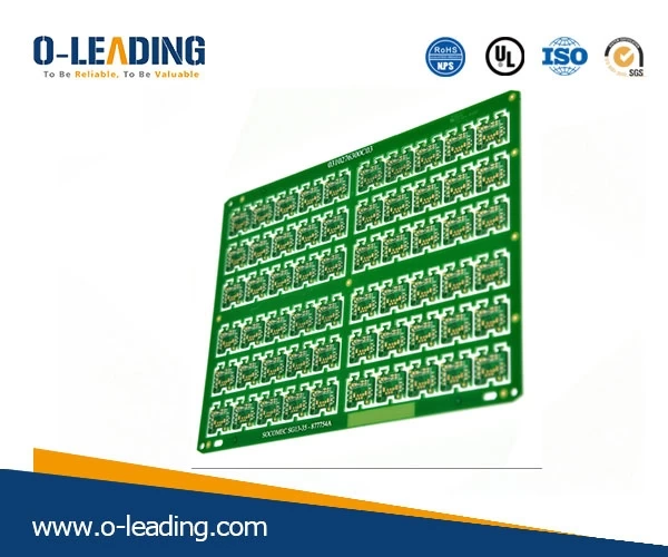
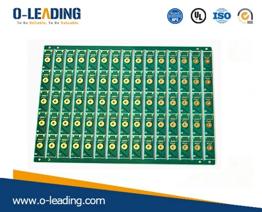
Double-layer PCB is the double-sided copper made by Double sided pcb supplier, and there is a metal hole, that is, there is copper on both sides, and there is copper in the hole, for the double-sided circuit board, the hole has copper is particularly important, because the earliest, the most difficult is the hole has copper (how to copper in the copper hole wall), this is to differentiate the double-sided, Single side of the most important basis. But the fake double PCB, Double Layers PCB only two sides have copper, but there is no copper in the hole, so there is no copper in the hole, Double Layers PCB but the double-sided pain of the circuit board, called the fake double PCB, looks like a double PCB.
PCB assembly Printed circuit board advantages (compared with Single-layer Board): Easy wiring, concise, wiring less labor intensity, line length is shorter.
Two-layer PCB design operation steps:
1, Prepare circuit schematic diagram
2, a new PCB file and loaded into the Components packaging library
3. Planning Circuit board
4. Loading network tables and components
5. Automatic layout of components
6. Layout adjustment
7. Network Density analysis
8, wiring rules set
9, automatic wiring
10, manual adjustment wiring
The improved structure of the Double-layer PCB includes a flexible circuit board body and a plurality of electronic components mounted on the positive and negative sides of the flexible PCB body. Double Layers PCB The first reinforcing plate and the second reinforcing plate are respectively arranged on the positive and negative sides of the flexible circuit board body, wherein the first reinforcing plate covers at least one of the electronic components mentioned, Double Layers PCB Or at least one for an electronic component to pass through; the second reinforcing plate covers at least one of the electronic components, or at least one of the electronic components to pass through.
There are wiring on both sides of the Double-layer PCB (double-sided boards). However, to use the two sides of the wire, you must have the appropriate circuit between the two sides to connect. The "bridge" between the circuits is called a guide hole (via). The guide hole is on the PCB, fills or spreads the metal the small hole, it may connect with the two sides the conductor. Because the two-tier PCB area is a lot larger than the single panel, Double Layers PCB and because the wiring can be interlaced with each other (can go around the other side), it is more suitable for more complex than the single panel on the circuit. In strict sense, the Double-layer PCB board is a very important PCB board, his use is very big, see a board PCB board is not a double PCB is also very simple, I believe that the Friends of the single panel of the understanding is completely can be grasped, Double Layers PCB double PCB is the extension of single-sided plate, It means that the wiring of the single-sided board is not enough to turn to the opposite side, and the two-layer PCB also has an important characteristic is the conduction hole. The simple point is two-sided walk line, both sides have the line! A word is: double-sided line of the board is a double PCB! Some friends will ask such as a board double-sided line, but only one side has electronic parts, such a board in the end is a double PCB or a single panel? The answer is obvious, such a board is a Double-layer circuit board, only on the board of the double board with a part on the plate. Multilayer circuit board to distinguish the PCB according to the number of wiring surface to determine the process of difficulty and processing prices, Double Layers PCB ordinary circuit board side-by-side line and double-sided line, commonly known as single-sided and Double-layer PCB, but high-end electronic products, due to product space design constraints, in addition to surface wiring, the interior can be superimposed multi-layer lines, production process, The production of each layer after the line, and then through the optical equipment positioning, compression, so that multi-layer lines superimposed on a led pcb board Printed circuit board.