ntroduction and troubleshooting of PCB nickel plating process
o-leading.com
o-leading.com
2017-07-09 12:13:10
function and characteristics
PCB (abbreviation for printed circuit boards in English PrintedCircuieBoard) uses nickel plated as the base coating for precious metals and base metals, and is also used as a surface layer for certain single-sided printed boards. For heavy duty wear surfaces such as switch contacts, contacts or plug gold, nickel is used as the base coating of the gold to improve wear resistance.
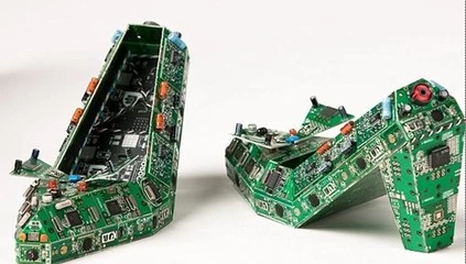
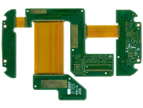
We often say that PCB nickel plated, bright nickel and dumb nickel (also called low stress nickel or semi bright nickel) usually require uniform and fine coating, low porosity, low stress and good ductility.
PCB (abbreviation for printed circuit boards in English PrintedCircuieBoard) uses nickel plated as the base coating for precious metals and base metals, and is also used as a surface layer for certain single-sided printed boards. For heavy duty wear surfaces such as switch contacts, contacts or plug gold, nickel is used as the base coating of the gold to improve wear resistance.

When used as a barrier, nickel can effectively prevent the diffusion of copper and other metals. Dumb nickel / gold composite coating is often used as an etching resistant metallic coating, and can adapt to the hot pressure welding and braze welding, only read only nickel can be used as anti-corrosive coating of ammonia etchant, without hot welding and bright coating PCB, commonly used light nickel / gold plating. Nickel coating thickness is generally not less than 2.5 microns, usually 4-5 microns.

PCB deposited layer of low stress nickel is usually plated with modified nickel metal nickel plating solution and some amino sulfonic acid nickel plating solution with additive of reducing stress.
We often say that PCB nickel plated, bright nickel and dumb nickel (also called low stress nickel or semi bright nickel) usually require uniform and fine coating, low porosity, low stress and good ductility.

